TB7102F Overview
1 2 3 4 5 6 7 8 Symbol PGND VIN EN SGND N.C. VFB LX Description Ground for the output section Input pin This pin is placed in the standby state if VENB = low. Standby current is 1 μA or less.
TB7102F Key Features
- Enables up to 1 A of load current (IOUT) with a minimum of external ponents
- High efficiency (η = 95% typ.) (@VIN = 5 V, VOUT = 3.3 V and IOUT = 300 mA)
- Operating voltage (VIN) range: 2.7 V to 5.5 V
- A high 1-MHz oscillation frequency (typ.) allows the use of small external ponents
- Uses internal phase pensation to achieve high efficiency with a minimum of external ponents
- Allows the use of a small surface-mount ceramic capacitor as an output filter capacitor
- Housed in a small surface-mount package (PS-8) with low thermal resistance
- Undervoltage lockout (UVLO), thermal shutdown (TSD) and overcurrent protection (OCP)
- The dot (-
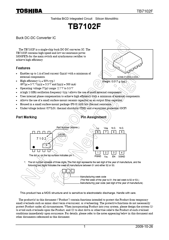
) on the top surface indicates pin 1
- The lot number consists of three digits. The first digit represents the last digit of the year of manufacture, and the f