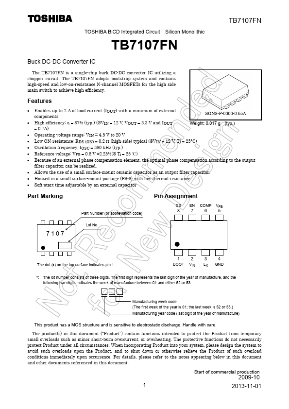
Datasheet4U Logo Datasheet4U.com

TB7107FN - Buck DC-DC Converter

Description

Pin No.

Bootstrap pin This pin is connected to Bootstrap capacitor.

A 0.1 μF bootstrap capacitor is required between BOOT pin and LX pin.

Features

  • Enables up to 2 A of load current (IOUT) with a minimum of external components. SON8-P-0303-0.65A.
  • High efficiency: η = 87% (typ. ) (@VIN = 12 V, VOUT = 3.3 V and IOUT = 0.7A) Weight: 0.017 g (typ. ).
  • Operating voltage range: VIN = 4.5 V to 20 V.
  • Low ON-resistance: RDS (ON) = 0.2 Ω (high-side) typical (@VIN = 12 V, Tj = 25°C).
  • Oscillation frequency: fOSC = 380 kHz (typ. ).
  • Reference voltage: VFB = 0.8 V ±2.25%(@ Tj = 25 ℃).
  • Be.

📥 Download Datasheet

Datasheet preview – TB7107FN

Datasheet Details

Part number TB7107FN
Manufacturer Toshiba
File Size 345.08 KB
Description Buck DC-DC Converter
Datasheet download datasheet TB7107FN Datasheet
Additional preview pages of the TB7107FN datasheet.
Other Datasheets by Toshiba

Full PDF Text Transcription

Click to expand full text
TOSHIBA BiCD Integrated Circuit Silicon Monolithic TB7107FN TB7107FN Buck DC-DC Converter IC The TB7107FN is a single-chip buck DC-DC converter IC utilizing a chopper circuit. The TB7107FN adopts bootstrap system and contains high-speed and low-on-resistance N-channel MOSFETs for the high side main switch to achieve high efficiency. Features • Enables up to 2 A of load current (IOUT) with a minimum of external components. SON8-P-0303-0.65A • High efficiency: η = 87% (typ.) (@VIN = 12 V, VOUT = 3.3 V and IOUT = 0.7A) Weight: 0.017 g (typ.) • Operating voltage range: VIN = 4.5 V to 20 V • Low ON-resistance: RDS (ON) = 0.2 Ω (high-side) typical (@VIN = 12 V, Tj = 25°C) • Oscillation frequency: fOSC = 380 kHz (typ.) • Reference voltage: VFB = 0.8 V ±2.
Published: |