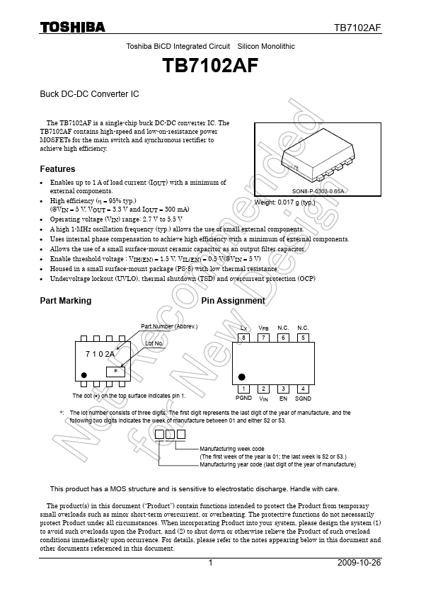
TB7102AF
Overview
- Enables up to 1 A of load current (IOUT) with a minimum of external components.
- High efficiency (η = 95% typ.) (@VIN = 5 V, VOUT = 3.3 V and IOUT = 300 mA) Weight: 0.017 g (typ.)
- Operating voltage (VIN) range: 2.7 V to 5.5 V
- A high 1-MHz oscillation frequency (typ.) allows the use of small external components.
- Uses internal phase compensation to achieve high efficiency with a minimum of external components.
- Allows the use of a small surface-mount ceramic capacitor as an output filter capacitor.
- Enable threshold voltage : VIH(EN) = 1.5 V, VIL(EN) = 0.5 V(@VIN = 5 V)
- Housed in a small surface-mount package (PS-8) with low thermal resistance.
- Undervoltage lockout (UVLO), thermal shutdown (TSD) and overcurrent protection (OCP) Part Marking