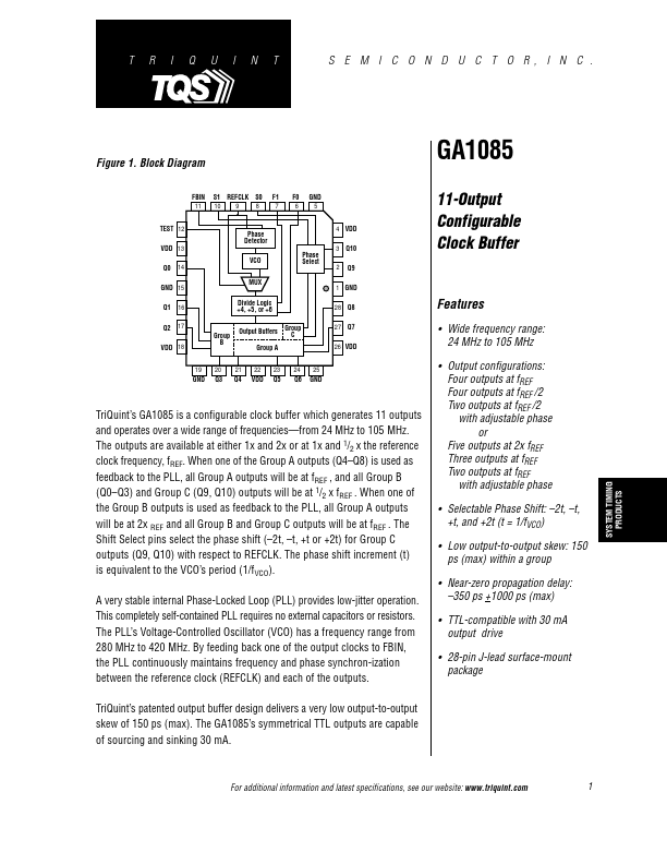
Datasheet4U Logo Datasheet4U.com

GA1085 - 11-Output Configurable Clock Buffer

Description

The core of the GA1085 is a Phase-Locked Loop (PLL) that continuously compares the reference clock (REFCLK) to the feedback clock (FBIN), maintaining a zero frequency difference between the two.

Q8) is always connected to FBIN, the PLL keeps the propagation delay

Features

  • Wide frequency range: 24 MHz to 105 MHz.
  • Output configurations: Four outputs at fREF Four outputs at fREF /2 Two outputs at fREF /2 ␣ ␣ ␣ ␣ with adjustable phase ␣ ␣ ␣ ␣ ␣ ␣ ␣ ␣ ␣ ␣ ␣ or Five outputs at 2x fREF Three outputs at fREF Two outputs at fREF ␣ ␣ ␣ ␣ with adjustable phase.
  • Selectable Phase Shift:.
  • 2t,.
  • t, +t, and +2t (t = 1/fVCO).
  • Low output-to-output skew: 150 ps (max) within a group.
  • Near-zero propagation delay:.
  • 3.

📥 Download Datasheet

Datasheet preview – GA1085

Datasheet Details

Part number GA1085
Manufacturer TriQuint Semiconductor
File Size 204.10 KB
Description 11-Output Configurable Clock Buffer
Datasheet download datasheet GA1085 Datasheet
Additional preview pages of the GA1085 datasheet.
Other Datasheets by TriQuint Semiconductor

Full PDF Text Transcription

Click to expand full text
T R I Q U I N T S E M I C O N D U C T O R, I N C . Figure 1.
Published: |