Datasheet4U Logo Datasheet4U.com

GA1086 - 11-Output Clock Buffer

Description

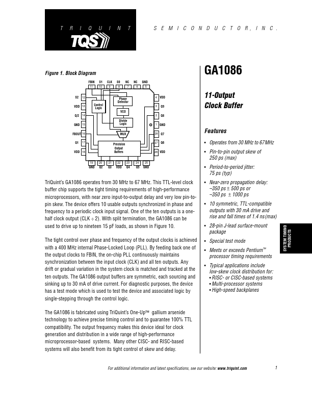
The GA1086 generates 10 outputs (Q1

Q9 and FBOUT) which have the same frequency and zero phase delay relative to the reference clock input.

In addition, there is one output (Q/2) that has 1/2 the frequency of the reference clock.

Features

  • Operates from 30 MHz to 67MHz.
  • Pin-to-pin output skew of 250 ps (max).
  • Period-to-period jitter: 75 ps (typ).
  • Near-zero propagation delay:.
  • 350 ps ± 500 ps or.
  • 350 ps ± 1000 ps.
  • 10 symmetric, TTL-compatible outputs with 30 mA drive and rise and fall times of 1.4 ns(max) SYSTEM TIMING.

📥 Download Datasheet

Datasheet preview – GA1086

Datasheet Details

Part number GA1086
Manufacturer TriQuint Semiconductor
File Size 234.88 KB
Description 11-Output Clock Buffer
Datasheet download datasheet GA1086 Datasheet
Additional preview pages of the GA1086 datasheet.
Other Datasheets by TriQuint Semiconductor

Full PDF Text Transcription

Click to expand full text
T R I Q U I N T S E M I C O N D U C T O R, I N C . Figure 1. Block Diagram FBIN 11 GA1086 S1 10 CLK 9 S0 8 NC 7 NC 6 GND 5 S2 12 VDD 13 Q/2 14 GND 15 FBOUT 16 Q1 17 Control Logic Phase Detector VCO 4 VDD 3 2 Q9 Q8 11-Output Clock Buffer Features • Operates from 30 MHz to 67MHz • Pin-to-pin output skew of 250 ps (max) • Period-to-period jitter: 75 ps (typ) • Near-zero propagation delay: –350 ps ± 500 ps or –350 ps ± 1000 ps • 10 symmetric, TTL-compatible outputs with 30 mA drive and rise and fall times of 1.4 ns(max) SYSTEM TIMING PRODUCTS Divide Logic MUX Precision Output Buffers 1 GND 28 27 Q7 Q6 VDD 18 26 VDD 19 20 21 22 23 24 25 GND Q2 Q3 VDD Q4 Q5 GND TriQuint’s GA1086 operates from 30 MHz to 67 MHz.
Published: |