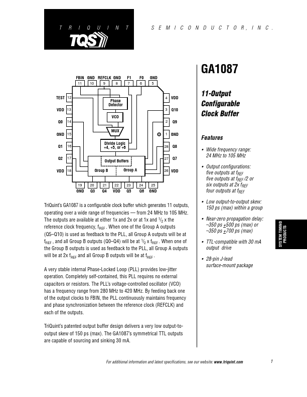
• Part: GA1087
  • Description: 11-Output Configurable Clock Buffer
  • Manufacturer: TriQuint Semiconductor
  • Size: 196.71 KB
Download GA1087 Datasheet PDF
TriQuint Semiconductor
GA1087
GA1087 is 11-Output Configurable Clock Buffer manufactured by TriQuint Semiconductor.
S E M I C O N D U C T O R, I N C . FBIN GND REFCLK GND 11 10 9 8 F1 F0 TEST 12 VDD 13 Phase Detector VCO 4 VDD 3 2 Q10 Q9 11-Output Configurable Clock Buffer Features - Wide frequency range: 24 MHz to 105 MHz - Output configurations: five outputs at f REF five outputs at f REF /2 or six outputs at 2x f REF four outputs at f REF - Low output-to-output skew: 150 ps (max) within a group SYSTEM TIMING PRODUCTS Q0 GND 15 Q1 Q2 16 17 MUX Divide Logic ÷4, ÷5, or ÷6 Output Buffers Group B Group A 1 GND 28 27 Q8 Q7 VDD 18 26 VDD Q3 Q4 Q5 Q6 Tri Quint’s GA1087 is a configurable clock buffer which generates 11 outputs, operating over a wide range of frequencies - from 24 MHz to 105 MHz. The outputs are available at either 1x and 2x or at 1x and 1/2 x the reference clock frequency, f REF . When one of the Group A outputs (Q5- Q10) is used as feedback to the PLL, all Group A outputs will be at f REF , and all Group B outputs (Q0- Q4) will be at 1/2 x f REF . When one of the Group B outputs is used as feedback to the PLL, all Group A outputs will be at 2x f REF and all Group B outputs will be at f REF . A very stable internal Phase-Locked Loop (PLL) provides low-jitter operation. pletely self-contained, this PLL requires no external capacitors or resistors. The PLL’s voltage-controlled oscillator (VCO) has a frequency range from 280 MHz to 420 MHz. By feeding back one of the output clocks to FBIN, the PLL continuously maintains frequency and phase synchronization between the reference clock (REFCLK) and each of the outputs. Tri Quint’s patented output buffer design delivers a very low output-tooutput skew of 150 ps (max). The GA1087’s symmetrical TTL outputs are capable of sourcing and sinking 30 m...