Datasheet4U.com
🌙
P1615ATFA Datasheet | UNIKC
Part:
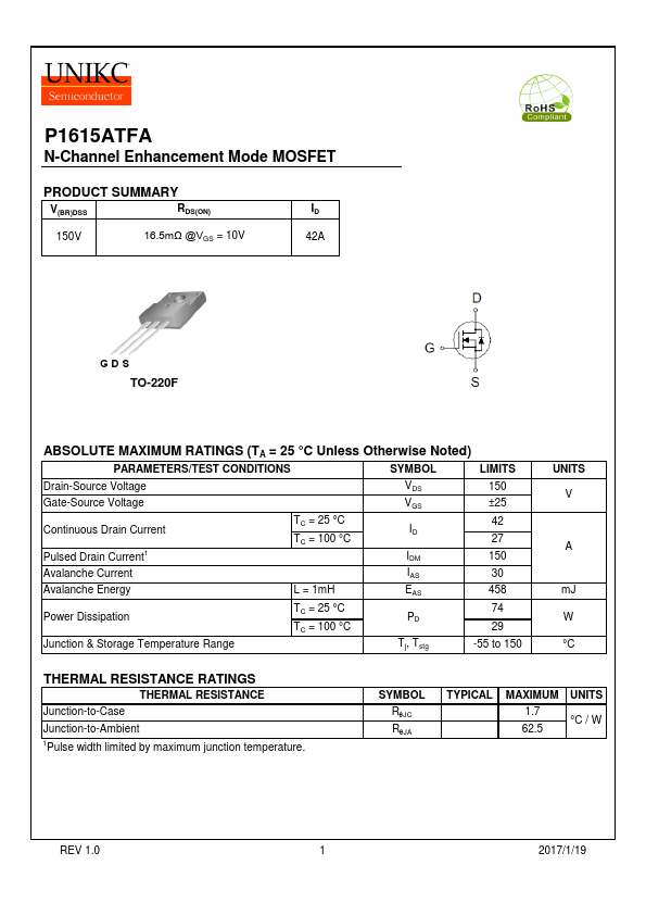
P1615ATFA
Description:
N-Channel MOSFET
Category:
MOSFET
Manufacturer:
UNIKC
Size:
770.76 KB
P1615ATFA Datasheet (PDF) Download
Related P1615ATFA Datasheets
P1615ATA N-Channel MOSFET
P1610ATF N-Channel MOSFET
P1610AT N-Channel MOSFET
UNIKC
P1615ATFA
Key Features
因各家封装模具不同而外观略有所差异,不影响电性及Layout。
Datasheets by Manufacturer
Part Number
Manufacturer
Description
P1615ATA
NIKO-SEM
N-Channel Transistor
P1610ATF
NIKO-SEM
N-Channel Transistor
×
Close