P1820AD
Description
P1820AD N-Channel Enhancement Mode MOSFET PRODUCT SUMMARY V(BR)DSS RDS(ON) 200V 160mΩ @VGS = 10V ID 18A TO-252 ABSOLUTE MAXIMUM RATINGS (TA = 25 °C Unless Otherwise Noted) PARAMETERS/TEST CON...
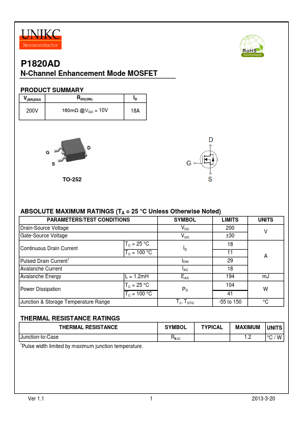
P1820AD N-Channel Enhancement Mode MOSFET PRODUCT SUMMARY V(BR)DSS RDS(ON) 200V 160mΩ @VGS = 10V ID 18A TO-252 ABSOLUTE MAXIMUM RATINGS (TA = 25 °C Unless Otherwise Noted) PARAMETERS/TEST CON...
| Part Number | Manufacturer | Description |
|---|---|---|
| P1820AD | NIKO-SEM | N-Channel Transistor |
| P1820HTFB | NIKO-SEM | N-Channel MOSFET |
| P1819 | Alliance Semiconductor | Low Power Mobile VGA EMI Reduction IC |
| P1822 | Alliance Semiconductor | Low Power Mobile VGA EMI Reduction IC |
| P1825HTFB | NIKO-SEM | N-Channel MOSFET |
| P1821 | Alliance Semiconductor | Low Power Mobile VGA EMI Reduction IC |
| P1818 | Alliance Semiconductor | Low Power Mobile VGA EMI Reduction IC |