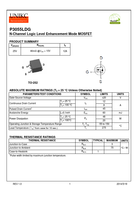
P3055LDG Overview
Key Features
- 55 to 150 275
| Part | P3055LDG |
|---|---|
| Description | N-Channel MOSFET |
| Category | MOSFET |
| Manufacturer | UNIKC |
| Size | 363.98 KB |
| Part Number | Manufacturer | Description |
|---|---|---|
| P3055LDG | Niko | N-Channel Logic Level Enhancement Mode Field Effect Transistor |
| P3055LD | Niko | N-Channel Logic Level Enhancement Mode Field Effect Transistor |
| P3055LSG | NIKO-SEM | N-Channel Field Effect Transistor |
| P3055LS | NIKO-SEM | N-Channel Logic Level Enhancement Mode Field Effect Transistor |
| P3055LTG | VBsemi | N-Channel 30V MOSFET |