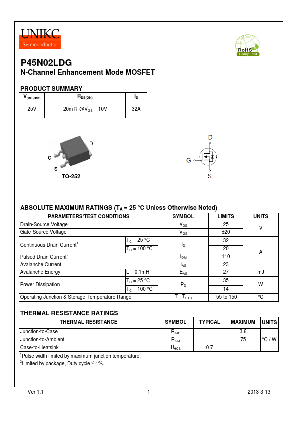
| Part | P45N02LDG |
|---|---|
| Description | N-Channel MOSFET |
| Category | MOSFET |
| Manufacturer | UNIKC |
| Size | 422.57 KB |
Pricing from 0.1848 USD, available from Win Source and RC Electronics.
Price & Availability
| Seller | Inventory | Price Breaks | Buy |
|---|---|---|---|
| Win Source | 50800 | 315+ : 0.1848 USD 760+ : 0.1525 USD 1175+ : 0.1478 USD 1615+ : 0.1432 USD |
View Offer |
| RC Electronics | 85731 | 1+ : 0.06 USD 10+ : 0.05 USD 100+ : 0.05 USD 1000+ : 0.05 USD |
View Offer |
Related Datasheets
| Part Number | Manufacturer | Description |
|---|---|---|
| P45N02LDG | Niko-Sem | N-Channel Logic Level Enhancement Mode Field Effect Transistor |
| P45N02LD | Niko-Sem | N-Channel Logic Level Enhancement Mode Field Effect Transistor |
| P45N02 | Intersil | 45A / 20V / 0.022 Ohm / N-Channel Logic Level Power MOSFETs |
| 45N03LTG | Niko | P45N03LTG |
| P45N03LTG | Niko | N-Channel Logic Level Enhancement Mode Field Effect Transistor |
