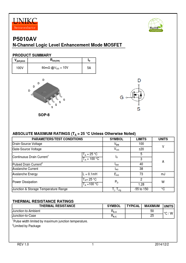
P5010AV Overview
| Part | P5010AV |
|---|---|
| Description | N-Channel MOSFET |
| Category | MOSFET |
| Manufacturer | UNIKC |
| Size | 465.91 KB |
| Part Number | Manufacturer | Description |
|---|---|---|
| P5010 | NXP Semiconductors | QorIQ integrated communication processor |
| KEH-P5010R | Pioneer | Cassette Player with RDS Tuner |
| KEH-P5011 | Pioneer | Cassette Player with Tuner |