Datasheet Summary
2SJ350-VB
2SJ350-VB Datasheet P-Channel 100 V (D-S) MOSFET
.VBsemi.
PRODUCT SUMMARY
VDS (V)
RDS(on) (Ω)
- 100
0.220 at VGS =
- 10 V 0.230 at VGS =
- 4.5 V
ID (A)
- 12
- 10
Qg (Typ.) 11.7
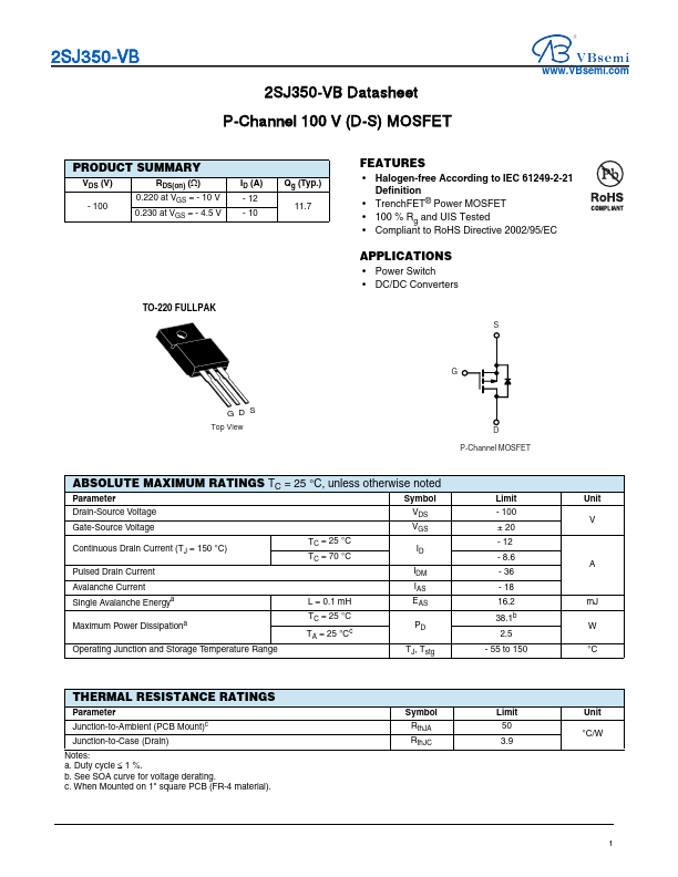
TO-220 FULLPAK
Features
- Halogen-free According to IEC 61249-2-21
Definition
- TrenchFET® Power MOSFET
- 100 % Rg and UIS Tested
- pliant to RoHS Directive 2002/95/EC
APPLICATIONS
- Power Switch
- DC/DC Converters
GDS Top View
D P-Channel...