SQS414CENW
SQS414CENW is Automotive N-Channel 60V MOSFET manufactured by Vishay.
FEATURES
- Trench FET® power MOSFET
- AEC-Q101 qualified
- 100 % Rg and UIS tested
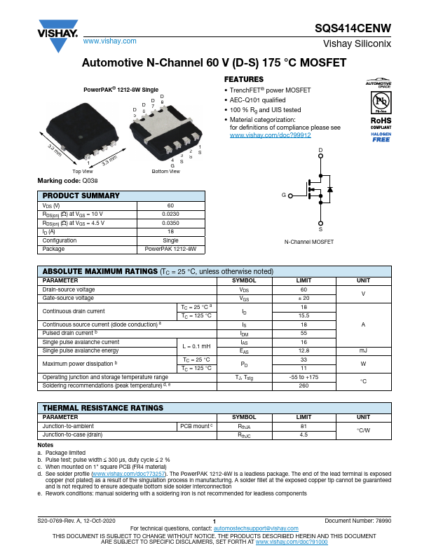
- Material categorization: for definitions of pliance please see .vishay./doc?99912
S N-Channel MOSFET
ABSOLUTE MAXIMUM RATINGS (TC = 25 °C, unless otherwise noted)
PARAMETER
SYMBOL
Drain-source voltage Gate-source voltage
Continuous drain current
Continuous source current (diode conduction) a Pulsed drain current b Single pulse avalanche current Single pulse avalanche energy
Maximum power dissipation b
Operating junction and storage temperature range Soldering remendations (peak temperature) d, e
TC = 25 °C a TC = 125 °C
L = 0.1 m H TC = 25 °C TC = 125 °C
VDS VGS
IS IDM IAS EAS
TJ, Tstg
LIMIT 60 ± 20 18 15.5 18 55 16 12.8 33 11
-55 to +175 260
UNIT V
A m J W °C
THERMAL RESISTANCE RATINGS
PARAMETER Junction-to-ambient Junction-to-case (drain)
PCB mount c
SYMBOL Rth JA Rth JC
LIMIT 81 4.5
UNIT °C/W
Notes a. Package limited b. Pulse test; pulse width 300 μs, duty cycle 2 % c. When mounted on 1" square PCB (FR4 material) d. See solder profile (.vishay./doc?73257). The Power PAK 1212-8W is a leadless package. The end of the lead terminal is exposed copper (not plated) as a result of the singulation process in manufacturing. A solder fillet at the exposed copper tip cannot be guaranteed and is not required to ensure adequate bottom side solder interconnection e. Rework conditions: manual soldering with a soldering iron is not remended for leadless ponents
S20-0769-Rev. A, 12-Oct-2020
Document Number: 78990
For technical questions, contact: automostechsupport@vishay.
THIS DOCUMENT IS SUBJECT TO CHANGE WITHOUT NOTICE. THE PRODUCTS DESCRIBED HEREIN AND THIS DOCUMENT ARE SUBJECT TO SPECIFIC DISCLAIMERS, SET FORTH AT .vishay./doc?91000
.vishay....