Si5442DU Overview
Key Specifications
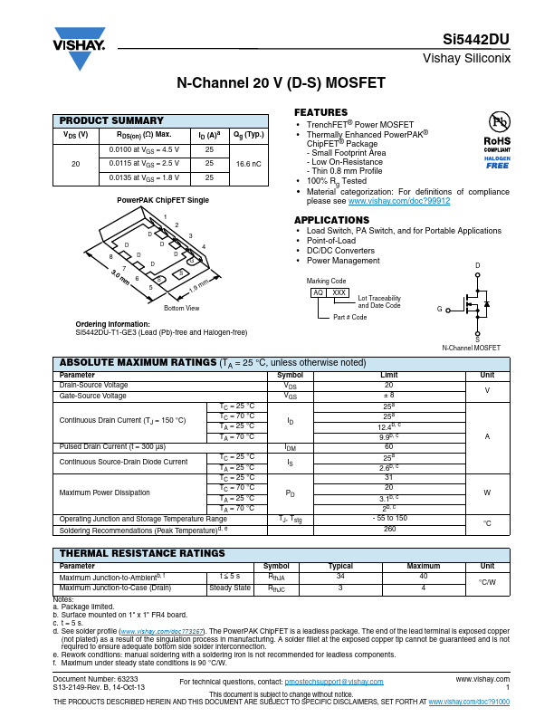
Mount Type: Surface Mount
Pins: 8
Height: 900 µm
Max Operating Temp: 150 °C
Key Features
- TrenchFET® Power MOSFET
- Thermally Enhanced PowerPAK® ChipFET® Package
- Small Footprint Area
- Low On-Resistance
- Thin 0.8 mm Profile