Datasheet Summary
.vishay.
Vishay General Semiconductor
Dual High-Voltage Trench MOS Barrier Schottky Rectifier
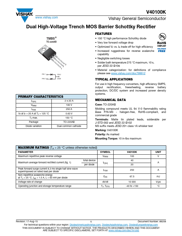
TMBS ®
TO-220AB
PIN 1 PIN 3
3 2 1
PIN 2 CASE
PRIMARY CHARACTERISTICS
IF(AV) VRRM IFSM VF at IF = 20 A at TJ = 125 °C TJ max. Package
2 x 20 A 100 V 250 A 0.63 V 150 °C
TO-220AB
Diode variation
Dual mon cathode
Features
- 150 °C high performance Schottky diode
- Very low forward voltage drop
- Optimized VF vs. IR trade off for high efficiency
- Increased ruggedness for reverse avalanche capability
- Negligible switching losses
- Solder bath temperature 275 °C maximum, 10 s, per JESD 22-B106
- Material categorization: for definitions of pliance please see...