Click to expand full text
WFSA5510
N- Channel and P-Channel Silicon MOSFETs
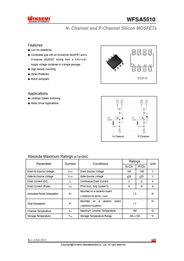
Features
■ Low On resistance. ■ Composite type with an N-channel MOSFET and a
P-channel MOSFET driving from a 4.5V/-4.5V supply voltage contained in a single package.
■ High-density mounting. ■ Zener-Protected ■ RoHS compliant.
SOP-8
Applications
■ Ultrahigh Speed Switching, ■ Motor Driver Applications
www.DataSheet.co.kr
Absolute Maximum Ratings at Ta=250C
Parameter
Drain-to-Source Voltage Gate-to-Source Voltage Drain Current (DC) Drain Current (Pulse) Allowable Power Dissipation
Symbol
VDSS VGSS ID IDP PD
Conditions
Drain-Source Voltage Gate-Source Voltage Continuous Drain Current PW≤10uS, duty cycle≤1% Mounted on a ceramic board (1000mm2×0.8mm) 1unit Mounted on a ceramic board
Ratings N-Ch
100 +20 2 8 1.