ZVN2120A Overview
Key Specifications
Package: TO-92-3
Mount Type: Through Hole
Max Operating Temp: 150 °C
Min Operating Temp: -55 °C
Key Features
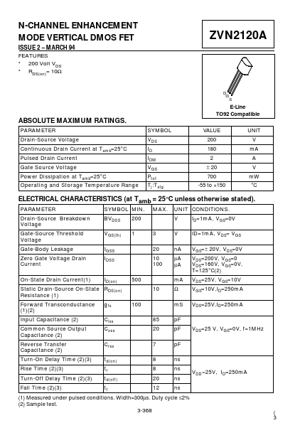
- * 200 Volt VDS * RDS(on)= 10Ω ZVN2120A D G S E-Line TO92 Compatible
| Part | ZVN2120A |
|---|---|
| Description | N-CHANNEL ENHANCEMENT MODE VERTICAL DMOS FET |
| Manufacturer | Zetex Semiconductors |
| Size | 45.81 KB |
Package: TO-92-3
Mount Type: Through Hole
Max Operating Temp: 150 °C
Min Operating Temp: -55 °C
| Seller | Inventory | Price Breaks | Buy |
|---|---|---|---|
| Win Source | 5 | 120+ : 0.418 USD 295+ : 0.343 USD 455+ : 0.3323 USD 625+ : 0.3216 USD |
View Offer |
| Worldway Electronics | 24775 | 7+ : 0.0716 USD 10+ : 0.0701 USD 100+ : 0.068 USD 500+ : 0.0658 USD |
View Offer |
| Part Number | Manufacturer | Description |
|---|---|---|
| CBT3253 | Nexperia | Dual 1-of-4 FET multiplexer/demultiplexer |
| TL074C | STMicroelectronics | LOW NOISE J-FET QUAD OPERATIONAL AMPLIFIER |
| CBT3125 | Nexperia | Quadruple FET bus switch |