ZVN2120C Overview
Key Specifications
Package: TO-92-3
Height: 4.01 mm
Length: 4.77 mm
Width: 2.41 mm
Key Features
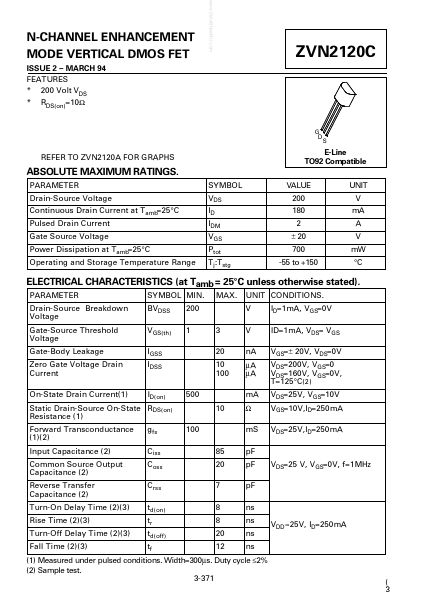
- * 200 Volt VDS * RDS(on)=10Ω ZVN2120C G D S REFER TO ZVN2120A FOR GRAPHS
| Part | ZVN2120C |
|---|---|
| Description | N-CHANNEL ENHANCEMENT MODE VERTICAL DMOS FET |
| Manufacturer | Zetex Semiconductors |
| Size | 70.54 KB |
Package: TO-92-3
Height: 4.01 mm
Length: 4.77 mm
Width: 2.41 mm
| Seller | Inventory | Price Breaks | Buy |
|---|---|---|---|
| No distributor offers were returned for this part. | |||
| Part Number | Manufacturer | Description |
|---|---|---|
| CBT3253 | Nexperia | Dual 1-of-4 FET multiplexer/demultiplexer |
| TL074C | STMicroelectronics | LOW NOISE J-FET QUAD OPERATIONAL AMPLIFIER |
| CBT3125 | Nexperia | Quadruple FET bus switch |