ZVN2120G Overview
Key Specifications
Package: SOT-223
Mount Type: Surface Mount
Pins: 4
Height: 1.65 mm
Key Features
- 200V * RDS(ON)
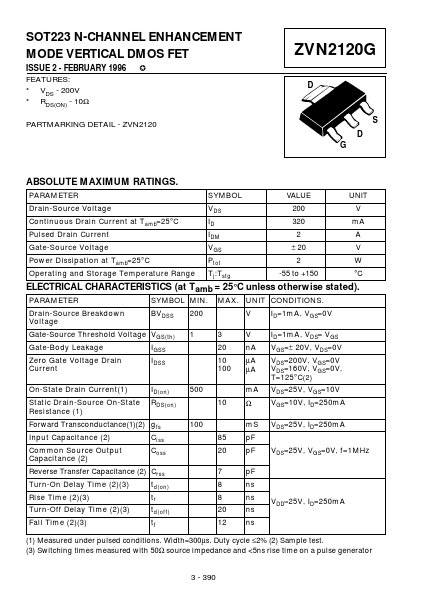
- 10Ω 7 ZVN2120G D PARTMARKING DETAIL
- ZVN2120 D G S
| Part | ZVN2120G |
|---|---|
| Description | N-CHANNEL ENHANCEMENT MODE VERTICAL DMOS FET |
| Manufacturer | Zetex Semiconductors |
| Size | 40.43 KB |
Package: SOT-223
Mount Type: Surface Mount
Pins: 4
Height: 1.65 mm
| Seller | Inventory | Price Breaks | Buy |
|---|---|---|---|
| Avnet | 1000 | 1000+ : 0.37538 USD 2000+ : 0.36225 USD 4000+ : 0.357 USD 8000+ : 0.35175 USD |
View Offer |
| Newark | 1000 | 1000+ : 0.514 USD | View Offer |
| Part Number | Manufacturer | Description |
|---|---|---|
| CBT3253 | Nexperia | Dual 1-of-4 FET multiplexer/demultiplexer |
| TL074C | STMicroelectronics | LOW NOISE J-FET QUAD OPERATIONAL AMPLIFIER |
| CBT3125 | Nexperia | Quadruple FET bus switch |