ZVNL120A Overview
Key Specifications
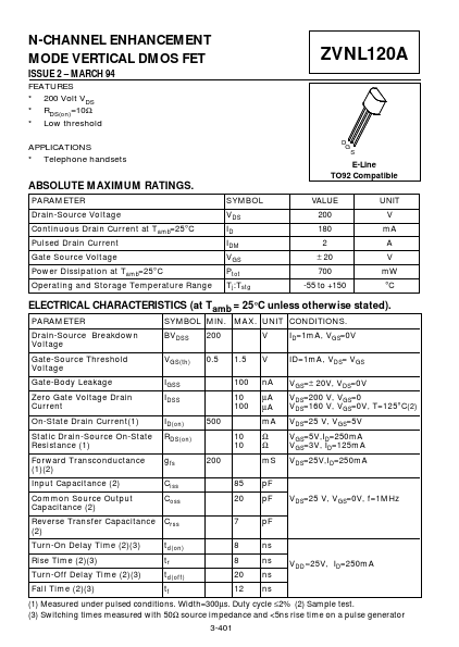
Package: TO-92-3
Mount Type: Through Hole
Pins: 3
Height: 4.01 mm
Key Features
- MARCH 94 FEATURES * 200 Volt VDS * RDS(on)=10Ω * Low threshold APPLICATIONS * Telephone handsets
- Drain Source Voltage (Volts)
| Part | ZVNL120A |
|---|---|
| Description | N-CHANNEL ENHANCEMENT MODE VERTICAL DMOS FET |
| Manufacturer | Zetex Semiconductors |
| Size | 49.95 KB |
Package: TO-92-3
Mount Type: Through Hole
Pins: 3
Height: 4.01 mm
| Seller | Inventory | Price Breaks | Buy |
|---|---|---|---|
| DigiKey | 1803 | 1+ : 1.27 USD 10+ : 0.799 USD 100+ : 0.5259 USD 500+ : 0.40826 USD |
View Offer |
| TME | 2745 | 1+ : 1.092 EUR 10+ : 0.703 EUR 100+ : 0.465 EUR 500+ : 0.361 EUR |
View Offer |
| Part Number | Manufacturer | Description |
|---|---|---|
| ZVNL120G | Diodes Incorporated | 200V N-CHANNEL ENHANCEMENT MODE MOSFET |