ZVP3310 Overview
Key Specifications
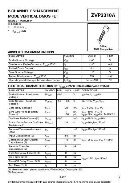
Package: TO-92-3
Mount Type: Through Hole
Pins: 3
Height: 4.01 mm
Key Features
- * 100 Volt VDS * RDS(on)=20Ω ZVP3310A D G S
| Part | ZVP3310 |
|---|---|
| Description | P-CHANNEL ENHANCEMENT MODE VERTICAL DMOS FET |
| Manufacturer | Zetex Semiconductors |
| Size | 82.78 KB |
Package: TO-92-3
Mount Type: Through Hole
Pins: 3
Height: 4.01 mm
| Seller | Inventory | Price Breaks | Buy |
|---|---|---|---|
| Avnet | 28000 | 4000+ : 0.23407 USD 8000+ : 0.23288 USD 16000+ : 0.23169 USD 32000+ : 0.23049 USD |
View Offer |
| Newark | 1409 | 1+ : 1.2 USD 10+ : 0.796 USD 25+ : 0.719 USD 50+ : 0.642 USD |
View Offer |
| Part Number | Manufacturer | Description |
|---|---|---|
| CBT3253 | Nexperia | Dual 1-of-4 FET multiplexer/demultiplexer |
| TL074C | STMicroelectronics | LOW NOISE J-FET QUAD OPERATIONAL AMPLIFIER |
| CBT3125 | Nexperia | Quadruple FET bus switch |