ZXMN6A11DN8
ZXMN6A11DN8 is 60V N-Channel MOSFET manufactured by Zetex Semiconductors.
DESCRIPTION
ID= 2.7A
This new generation of TRENCH MOSFETs from Zetex utilises a unique structure that bines the benefits of low on-resistance with fast switching speed. This makes them ideal for high efficiency, low voltage, power management applications.
FEATURES
- Low on-resistance
- Fast switching speed
- Low threshold
- Low gate drive
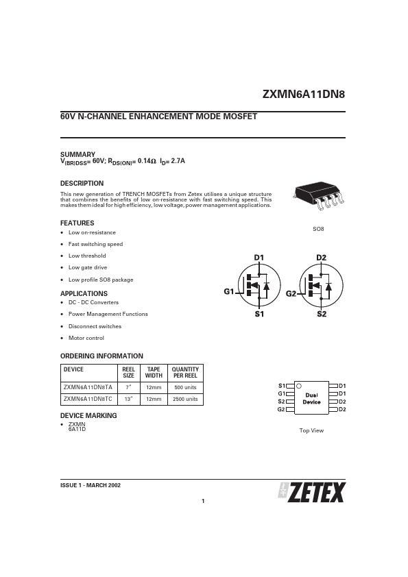
- Low profile SO8 package
SO8
APPLICATIONS
- DC
- DC Converters
- Power Management Functions
- Disconnect switches
- Motor control
ORDERING INFORMATION
DEVICE ZXMN6A11DN8TA ZXMN6A11DN8TC REEL SIZE 7” 13” TAPE WIDTH 12mm 12mm QUANTITY PER REEL 500 units 2500 units
DEVICE MARKING
- ZXMN
6A11D Top View
ISSUE 1
- MARCH 2002 1
ABSOLUTE MAXIMUM RATINGS
PARAMETER Drain-Source Voltage Gate Source Voltage Continuous Drain Current V GS =10V; T A =25°C(b) V GS =10V; T A =70°C(b) V GS =10V; T A =25°C(a) Pulsed Drain Current (c) Continuous Source Current (Body Diode) (b) Pulsed Source Current (Body Diode)(c) Power Dissipation at T A =25°C (a)(d) Linear Derating Factor Power Dissipation at T A =25°C (a)(e) Linear Derating Factor Power Dissipation at T A =25°C (b)(d) Linear Derating Factor Operating and Storage Temperature Range SYMBOL V DSS V GS ID LIMIT 60 Ϯ20 2.7 2.2 2.1 8.3 3.2 8.3 1.25 10 1.8 14 2.1 17 -55 to +150 UNIT V V A
I DM IS I SM PD PD PD T j :T stg
A A A m W m W/°C m W m W/°C m W m W/°C °C
THERMAL RESISTANCE
PARAMETER Junction to Ambient (a)(d) Junction to Ambient (a)(e) Junction to Ambient (b)(d) SYMBOL R θ JA R θ JA R θ JA VALUE 100 70 60 UNIT °C/W °C/W °C/W
NOTES (a) For a device surface mounted on 25mm x 25mm FR4 PCB with high coverage of single sided 1oz copper, in still air conditions (b) For a device surface mounted on FR4 PCB measured at tр10 secs. (c) Repetitive rating 25mm x 25mm FR4 PCB, D=0.05 pulse width=10µs
- pulse width limited by maximum junction temperature. (d) For device with one active die (e) For device with two active die running at equal power.
ISSUE 1
- MARCH 2002...