ZXMP2120E5 Overview
Key Specifications
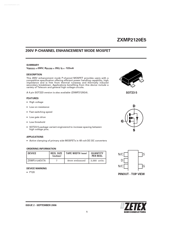
Package: SOT-23-5
Mount Type: Surface Mount
Pins: 5
Height: 1.3 mm
Key Features
- High voltage
- Low on-resistance
- Fast switching speed
- Low gate drive
- Low threshold
| Part | ZXMP2120E5 |
|---|---|
| Description | 200V P-CHANNEL ENHANCEMENT MODE MOSFET |
| Category | MOSFET |
| Manufacturer | Zetex Semiconductors |
| Size | 409.19 KB |
Package: SOT-23-5
Mount Type: Surface Mount
Pins: 5
Height: 1.3 mm
| Seller | Inventory | Price Breaks | Buy |
|---|---|---|---|
| RS (Formerly Allied Electronics) | 0 | 25+ : 1.77 USD 50+ : 1.73 USD 100+ : 1.5 USD 250+ : 1.33 USD |
View Offer |
| Win Source | 25800 | 180+ : 0.3269 USD 435+ : 0.268 USD 670+ : 0.2599 USD 920+ : 0.2518 USD |
View Offer |
| Part Number | Manufacturer | Description |
|---|---|---|
| ZXMP2120G4TA | Diodes Incorporated | 200V P-CHANNEL ENHANCEMENT MODE MOSFET |
| ZXMP2120G4TC | Diodes Incorporated | 200V P-CHANNEL ENHANCEMENT MODE MOSFET |
| ZXMP2120G4 | Diodes Incorporated | 200V P-CHANNEL ENHANCEMENT MODE MOSFET |