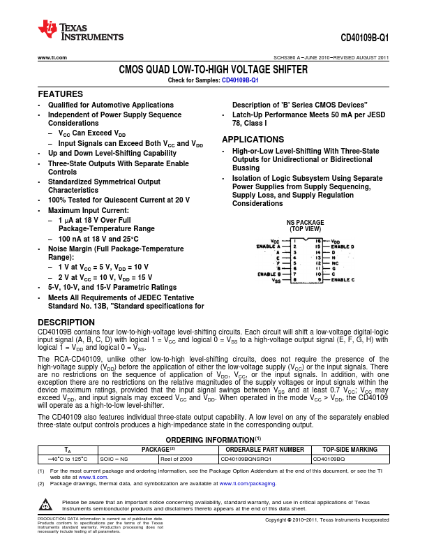
CD40109BQ
Overview
CD40109B contains four low-to-high-voltage level-shifting circuits. Each circuit will shift a low-voltage digital-logic input signal (A, B, C, D) with logical 1 = VCC and logical 0 = VSS to a high-voltage output signal (E, F, G, H) with logical 1 = VDD and logical 0 = VSS.
- Qualified for Automotive Applications
- Independent of Power Supply Sequence Considerations - VCC Can Exceed VDD - Input Signals can Exceed Both VCC and VDD
- Up and Down Level-Shifting Capability
- Three-State Outputs With Separate Enable Controls
- Standardized Symmetrical Output Characteristics
- 100% Tested for Quiescent Current at 20 V
- Maximum Input Current: - 1 µA at 18 V Over Full Package-Temperature Range - 100 nA at 18 V and 25°C
- Noise Margin (Full Package-Temperature Range): - 1 V at VCC = 5 V, VDD = 10 V - 2 V at VCC = 10 V, VDD = 15 V
- 5-V, 10-V, and 15-V Parametric Ratings
- Meets All Requirements of JEDEC Tentative Standard No. 13B, "Standard specifications for