Datasheet Summary
CDC203 3.3-V HEX INVERTER/CLOCK DRIVER
D Replaces 74AC11203 D Low-Skew Propagation Delay
Specifications for Clock Driver
Applications
D Operates at 3.3-V VCC D Flow-Through Architecture Optimizes
PCB Layout
D Center-Pin VCC and GND Pin
Configurations Minimize High-Speed
Switching Noise
D EPIC (Enhanced-Performance Implanted
CMOS) 1-µm Process
D 500-mA Typical Latch-Up Immunity at 125°C
D Packaged in Plastic Small-Outline Package
SCAS324A
- OCTOBER 1989
- REVISED NOVEMBER 1995
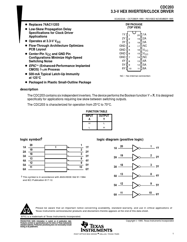
DW PACKAGE (TOP VIEW)
1Y 2Y 3Y GND GND GND GND 4Y 5Y 6Y
1 2 3 4 5 6 7 8 9 10
20 1A 19 2A 18 3A 17 NC 16 VCC 15 VCC 14 NC
13 4A
12 5A
11 6A
- No internal connection description
The CDC203 contains six...