Datasheet4U Logo Datasheet4U.com

CDCF5801 - CLOCK MULTIPLIER

Datasheet Summary

Description

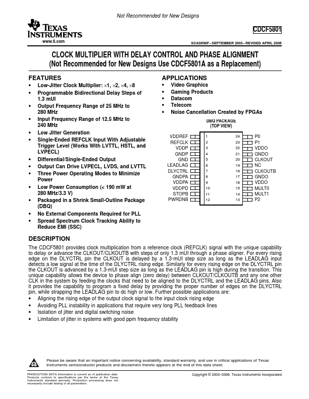
The CDCF5801 provides clock multiplication from a reference clock (REFCLK) signal with the unique capability to delay or advance the CLKOUT/CLKOUTB with steps of only 1.3 mUI through a phase aligner.

Features

  • Low-Jitter Clock Multiplier: ×1, ×2, ×4, ×8.
  • Programmable Bidirectional Delay Steps of 1.3 mUI.
  • Output Frequency Range of 25 MHz to 280 MHz.
  • Input Frequency Range of 12.5 MHz to 240 MHz.
  • Low Jitter Generation.
  • Single-Ended REFCLK Input With Adjustable Trigger Level (Works With LVTTL, HSTL, and LVPECL).
  • Differential/Single-Ended Output.
  • Output Can Drive LVPECL, LVDS, and LVTTL.
  • Three Power Operating Modes to Minimiz.

📥 Download Datasheet

Datasheet preview – CDCF5801

Datasheet Details

Part number CDCF5801
Manufacturer Texas Instruments
File Size 382.66 KB
Description CLOCK MULTIPLIER
Datasheet download datasheet CDCF5801 Datasheet
Additional preview pages of the CDCF5801 datasheet.
Other Datasheets by Texas Instruments

Full PDF Text Transcription

Click to expand full text
Not Recommended for New Designs CDCF5801 www.ti.com SCAS698F – SEPTEMBER 2003 – REVISED APRIL 2006 CLOCK MULTIPLIER WITH DELAY CONTROL AND PHASE ALIGNMENT (Not Recommended for New Designs Use CDCF5801A as a Replacement) FEATURES • Low-Jitter Clock Multiplier: ×1, ×2, ×4, ×8 • Programmable Bidirectional Delay Steps of 1.3 mUI • Output Frequency Range of 25 MHz to 280 MHz • Input Frequency Range of 12.5 MHz to 240 MHz • Low Jitter Generation • Single-Ended REFCLK Input With Adjustable Trigger Level (Works With LVTTL, HSTL, and LVPECL) • Differential/Single-Ended Output • Output Can Drive LVPECL, LVDS, and LVTTL • Three Power Operating Modes to Minimize Power • Low Power Consumption (< 190 mW at 280 MHz/3.
Published: |