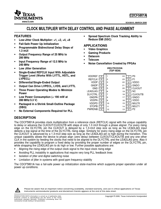
CDCF5801A Description
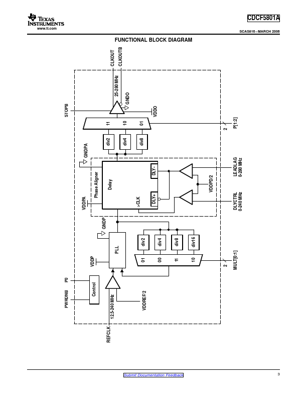
The CDCF5801A provides clock multiplication from a reference clock (REFCLK) signal with the unique capability to delay or advance the CLKOUT/CLKOUTB with steps of only 1.3 mUI through a phase aligner. For every rising edge on the DLYCTRL pin the CLKOUT is delayed by a 1.3-mUI step size as long as the LEADLAG input detects a low signal at the time of the DLYCTRL rising edge. Similarly for every rising edge on the...
CDCF5801A Key Features
- Low-Jitter Clock Multiplier: ×1, ×2, ×4, ×8
- Fail-Safe Power Up Initialization
- Output Frequency Range of 25 MHz to 280 MHz
- Input Frequency Range of 12.5 MHz to 240 MHz
- Low Jitter Generation
- Single-Ended REFCLK Input With Adjustable
- Differential/Single-Ended Output
- Output Can Drive LVPECL, LVDS, and LVTTL
- Three Power Operating Modes to Minimize
- Low Power Consumption (< 190 mW at 280 MHz/3.3 V)