CDCL6010
CDCL6010 is Clock Multiplier / Distributor / Jitter Cleaner/Buffer manufactured by Texas Instruments.
.ti.
SLLS780B
- FEBRUARY 2007
- REVISED MARCH 2011
1.8V, 11 Output Clock Multiplier, Distributor, Jitter Cleaner, and Buffer
Check for Samples: CDCL6010
Features
- 2 Single 1.8V Supply
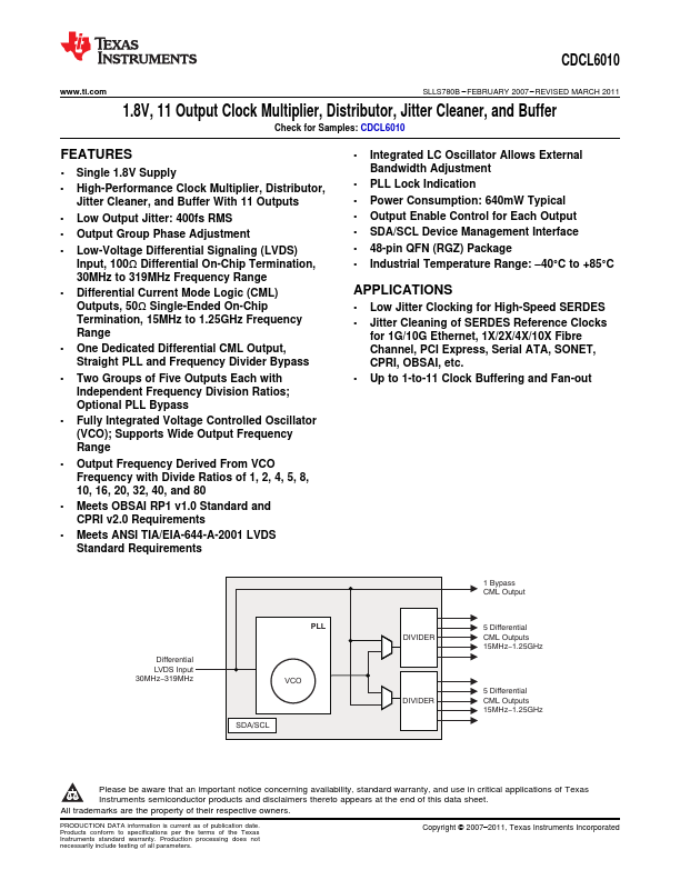
- High-Performance Clock Multiplier, Distributor, Jitter Cleaner, and Buffer With 11 Outputs
- Low Output Jitter: 400fs RMS
- Output Group Phase Adjustment
- Low-Voltage Differential Signaling (LVDS) Input, 100Ω Differential On-Chip Termination, 30MHz to 319MHz Frequency Range
- Differential Current Mode Logic (CML) Outputs, 50Ω Single-Ended On-Chip Termination, 15MHz to 1.25GHz Frequency Range
- One Dedicated Differential CML Output, Straight PLL and Frequency Divider Bypass
- Two...