Datasheet4U Logo Datasheet4U.com

CDCLVD1212 - 2:12 Low Additive Jitter LVDS Buffer

General Description

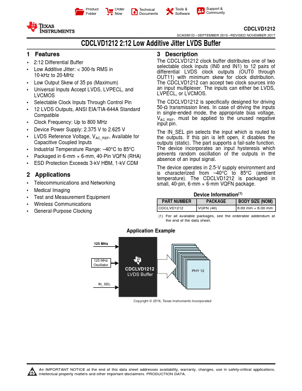
The CDCLVD1212 clock buffer distributes one of two selectable clock inputs (IN0 and IN1) to 12 pairs of differential LVDS clock outputs (OUT0 through OUT11) with minimum skew for clock distribution.

The CDCLVD1212 can accept two clock sources into an input multiplexer.

Key Features

  • 1 2:12 Differential Buffer.
  • Low Additive Jitter: < 300-fs RMS in 10-kHz to 20-MHz.
  • Low Output Skew of 35 ps (Maximum).
  • Universal Inputs Accept LVDS, LVPECL, and LVCMOS.
  • Selectable Clock Inputs Through Control Pin.
  • 12 LVDS Outputs, ANSI EIA/TIA-644A Standard Compatible.
  • Clock Frequency: Up to 800 MHz.
  • Device Power Supply: 2.375 V to 2.625 V.
  • LVDS Reference Voltage, VAC_REF, Available for Capacitive Coupled Inputs.

📥 Download Datasheet

Full PDF Text Transcription (Reference)

The following content is an automatically extracted verbatim text from the original manufacturer datasheet and is provided for reference purposes only.

View original datasheet text
Product Folder Order Now Technical Documents Tools & Software Support & Community CDCLVD1212 SCAS901D – SEPTEMBER 2010 – REVISED NOVEMBER 2017 CDCLVD1212 2:12 Low Additive Jitter LVDS Buffer 1 Features •1 2:12 Differential Buffer • Low Additive Jitter: < 300-fs RMS in 10-kHz to 20-MHz • Low Output Skew of 35 ps (Maximum) • Universal Inputs Accept LVDS, LVPECL, and LVCMOS • Selectable Clock Inputs Through Control Pin • 12 LVDS Outputs, ANSI EIA/TIA-644A Standard Compatible • Clock Frequency: Up to 800 MHz • Device Power Supply: 2.375 V to 2.