CDCUN1208LP
CDCUN1208LP is 400-MHz Low Power 2:8 Fan-Out Buffer manufactured by Texas Instruments.
Features
- 1 Supports PCIe Gen1, Gen2, Gen3
- Configuration Options (Through Pins or SPI/I2C):
- Input Type (HCSL, LVDS, LVCMOS)
- Output Type (HCSL, LVDS, LVCMOS)
- Signal Edge Rate (Slow, Medium, Fast)
- Clock Input Divide Value (/1, /2, /4, /8)
- IN2
Only
- Low-Power Consumption and Power Management
Features
, Including 1.8-V Operation and Output Enable Control
- Integrated Voltage Regulators to Improve PSNR
- Excellent Additive Jitter Performance
- 200 fs RMS (10 k Hz to 20 MHz), LVDS at
100 MHz
- 160 fs RMS (10 k Hz to 20 MHz), HCSL at
100 MHz
- Maximum Operating Frequency:
- Differential Mode: up to 400 MHz
- LVCMOS Mode: up to 250 MHz
- ESD Protection Exceeds 2-k V HBM, 500-V CDM
- Industrial Temperature Range (- 40°C to 85°C)
- Wide Supply Range (1.8 V, 2.5 V, or 3.3 V)
3 Description
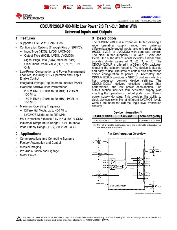
The CDCUN1208LP is a 2:8 fan-out buffer featuring a wide operating supply range, two universal differential/single-ended inputs, and universal outputs (HCSL, LVDS, or LVCMOS) with edge-rate control. The clock buffer supports PCIe Gen1, Gen2 and Gen3. One of the device inputs includes a divider that provides divide values of /1, /2, /4, or /8. The CDCUN1208LP is offered in a 32-pin QFN package, reducing the solution footprint. The device is flexible and easy to use. The state of certain pins determines device configuration at power up. Alternately, the CDCUN1208LP provides a SPI/I2C port with which a host processor controls device settings. The CDCUN1208LP delivers excellent additive jitter performance, and low power consumption. The output section includes four dedicated supply pins enabling the operation of output ports from different power supply domains. This provides the ability to clock devices switching at different LVCMOS levels without the need for external logic level translation circuitry.
Device Information(1)
PART NUMBER
PACKAGE
BODY SIZE (NOM)
VQFN (32)
5.00 mm × 5.00 mm
(1) For all available packages, see the orderable addendum at the end of the...