Datasheet4U Logo Datasheet4U.com

CSD18533KCS - 60V N-Channel power MOSFET

General Description

This 60V, 5.0mΩ, TO-220 NexFET™ power MOSFET is designed to minimize losses in power conversion applications.

SPACE Drain (Pin 2) Gate (Pin 1) Source (Pin 3) Product Summary TA = 25°C TYPICAL VALUE VDS Drain-to-source voltage 60 Qg Gate charge total (10V) 28 Qgd Gate charge gate-to-drain 3.9 
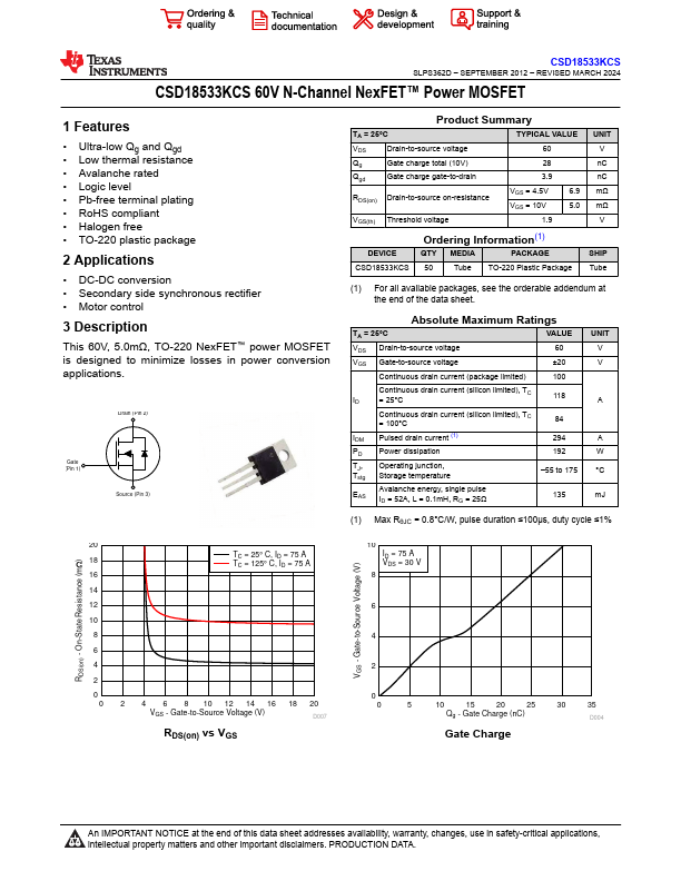
RDS(on) Drain-to-source on-resistance VGS = 4.5V VGS = 10V 6.9 5.0 VGS(th) Threshold voltage 1.9 UNIT V nC nC mΩ mΩ V DEVICE Ordering Information(1) QTY MEDIA PACKAGE SHIP CSD18533KCS 50 Tube TO-220 Plastic Package Tube (1) For all available packages, see the orderable addendum at the end of the data sheet.

Absolute Maximum Ratings TA = 25°C VDS Drain-to-source voltage VGS Gate-to-source voltage Continuous drain current (package limited) VALUE 60 ±20 100 Continuous drain current (silicon limited), TC ID = 25°C 118 Continuous drain current (silicon limited), TC = 100°C 84 IDM Pulsed drain current (1) PD Power dissipation TJ, Operating junction, Tstg Storage temperature EAS Avalanche energy, single pulse ID = 52A, L = 0.1mH, RG = 25Ω 294 192 –55 to 175 135 UNIT V V A A W °C mJ (1) Max RθJC = 0.8°C/W, pulse duration ≤100μs, duty cycle ≤1% RDS(on) - On-State Resistance (m:) VGS - Gate-to-Source Voltage (V) 20 18 TC = 25° C, ID = 75 A TC = 125° C, ID = 75 A 16 14 12 10 8 6 4 2 0 0 2 4 6 8 10 12 14 16 18 20 VGS - Gate-to-Source Voltage (V) D007 RDS(on) vs VGS 10 ID = 75 A VDS = 30 V 8 6 4 2 0 0 5 10 15 20 25 30 35 Qg - Gate Charge (nC) D004 Gate Charge An IMPORTANT NOTICE at the end of this data sheet addresses availability, warr

Overview

CSD18533KCS SLPS362D – SEPTEMBER 2012 – REVISED MARCH 2024 CSD18533KCS 60V N-Channel NexFET™ Power MOSFET.

Key Features

  • Ultra-low Qg and Qgd.
  • Low thermal resistance.
  • Avalanche rated.
  • Logic level.
  • Pb-free terminal plating.
  • RoHS compliant.
  • Halogen free.
  • TO-220 plastic package 2.