Datasheet4U Logo Datasheet4U.com

CSD18534Q5A - N-Channel MOSFET

General Description

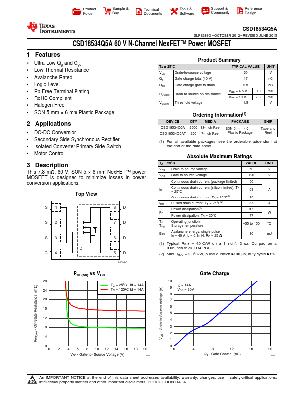
This 7.8 mΩ, 60 V, SON 5 × 6 mm NexFET™ power MOSFET is designed to minimize losses in power conversion applications.

Top View S1 8D S2 7D S3 G4 D 6D 5D P0093-01 Product Summary TA = 25°C VDS Drain-to-source voltage Qg Gate charge total (10 V) Qgd Gate charge gate-to-drain RDS(on) Drain-to-source on-resistance VGS(th) Threshold voltage TYPICAL VALUE 60 17 3.5 VGS = 4.5 V VGS = 10 V 1.9 9.9 7.8 UNIT V nC nC mΩ mΩ V Ordering Information(1) DEVICE QTY MEDIA PACKAGE CSD18534Q5A 2500 13-Inch Reel SON 5 mm × 6 mm CSD18534Q5AT 250 7-Inch Reel Plastic Package SHIP Tape and Reel (1) For all available packages, see the orderable addendum at the end of the data sheet.

Absolute Maximum Ratings TA = 25°C VDS Drain-to-source voltage VGS Gate-to-source voltage Continuous drain current (package limited) VALUE 60 ±20 50 UNIT V V ID Continuous drain current (silicon limited), TC = 25°C 69 Continuous drain current, TA = 25°C(1) IDM Pulsed drain current, TA = 25°C(2) Power dissipation(1) PD Power dissipation, TC = 25°C 13 229 3.1 77 TJ, Operating junction, Tstg Storage temperature –55 to 150 EAS Avalanche energy, single pulse ID = 40 A, L = 0.1mH, RG = 25 Ω 80 A A W °C mJ (1) Typical RθJA = 40°C/W on a 1 inch2, 2 oz.

Overview

Product Folder Sample & Buy Technical Documents Tools & Software Support & Community Reference Design CSD18534Q5A SLPS389D – OCTOBER 2012 – REVISED JUNE 2015 CSD18534Q5A 60 V N-Channel NexFET™ Power MOSFET.

Key Features

  • 1 Ultra-Low Qg and Qgd.
  • Low Thermal Resistance.
  • Avalanche Rated.
  • Logic Level.
  • Pb Free Terminal Plating.
  • RoHS Compliant.
  • Halogen Free.
  • SON 5 mm × 6 mm Plastic Package 2.