CSD25202W15T Overview
Key Specifications
Mount Type: Surface Mount
Pins: 9
Height: 625 µm
Length: 1.75 mm
Description
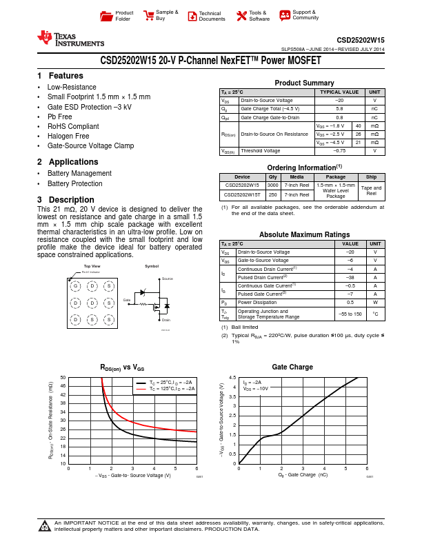
This 21 mΩ, 20 V device is designed to deliver the lowest on resistance and gate charge in a small 1.5 mm × 1.5 mm chip scale package with excellent Top View Pin A1 Indicator G D S Symbol Source Gate D D S D S S Drain P0117-01 Product Summary TA = 25°C VDS Drain-to-Source Voltage Qg Gate Charge Total (–4.5 V) Qgd Gate Charge Gate-to-Drain RDS(on) Drain-to-Source On Resistance VGS(th) Threshold Voltage TYPICAL VALUE –20 5.8 0.8 VGS = –1.8 V 40 VGS = –2.5 V 26 VGS = –4.5 V 21 –0.75 UNIT V nC nC mΩ mΩ mΩ V Device CSD25202W15 CSD25202W15T.
Key Features
- 1 Low-Resistance
- Small Footprint 1.5 mm × 1.5 mm
- Gate ESD Protection –3 kV
- RoHS Compliant
- Halogen Free