Datasheet4U Logo Datasheet4U.com

CSD86311W1723 Datasheet Dual N-Channel Power MOSFET

Manufacturer: Texas Instruments

Overview: CSD86311W1723 www.ti.com Dual N-Channel NexFET™ Power MOSFET Check for Samples: CSD86311W1723 SLPS251 – MAY.

General Description

The device has been designed to deliver the lowest on resistance and gate charge in the smallest outline possible with thermal characteristics in an ultra low profile.

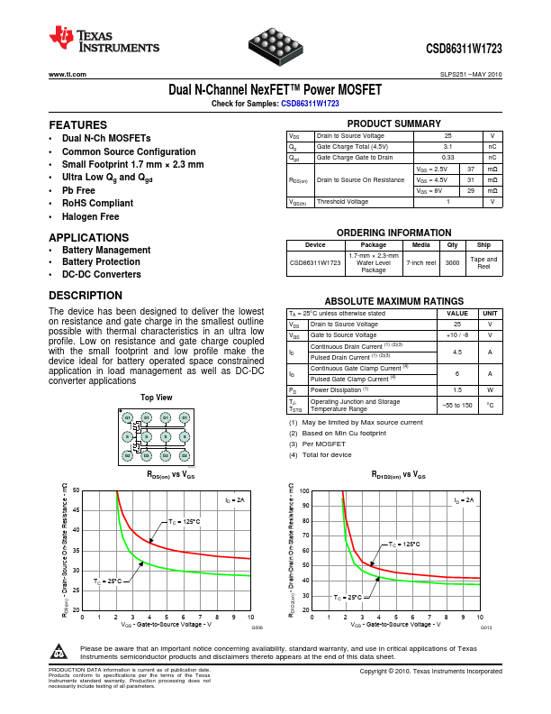
Low on resistance and gate charge coupled with the small footprint and low profile make the device ideal for battery operated space constrained application in load management as well as DC-DC converter applications Top View G1 D1 D1 D1 S S S S G2 D2 D2 D2 P0115-01 RDS(on) vs VGS 50 ID = 2A 45 TC = 125°C 40 35 30 TC = 25°C 25 20 0 1 2 3 4 5 6 7 8 9 10 VGS - Gate-to-Source Voltage - V G006 Text Added for Spacing ABSOLUTE MAXIMUM RATINGS TA = 25°C unless otherwise stated VDS Drain to Source Voltage VGS Gate to Source Voltage Continuous Drain Current (1) (2)(3) ID Pulsed Drain Current (1) (2)(3) Continuous Gate Clamp Current (4) IG Pulsed Gate Clamp Current (4) PD Power Dissipation (1) TJ, Operating Junction and Storage TSTG Temperature Range VALUE 25 +10 / -8 4.5 6 1.5 –55 to 150 (1) May be limited by Max source current (2) Based on Min Cu footprint (3) Per MOSFET (4) Total for device UNIT V V A A W °

Key Features

  • 1.
  • Dual N-Ch MOSFETs.
  • Common Source Configuration.
  • Small Footprint 1.7 mm × 2.3 mm.
  • Ultra Low Qg and Qgd.
  • Pb Free.
  • RoHS Compliant.
  • Halogen Free.