DS90CR286AT-Q1
Overview
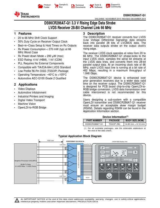
The DS90CR286AT-Q1 receiver converts four LVDS (Low Voltage Differential Signaling) data streams back into parallel 28 bits of LVCMOS data. The receiver data outputs strobe on the output clock's rising edge.
- 1 20 to 66 MHz Shift Clock Support
- 50% Duty Cycle on Receiver Output Clock
- Best-in-Class Setup & Hold Times on Rx Outputs
- Rx Power Consumption < 270 mW (typ) at 66 MHz Worst Case
- Rx Power-down Mode < 200 μW (max)
- ESD Rating: 4 kV (HBM), 1 kV (CDM)
- PLL Requires No External Components
- Compatible with TIA/EIA-644 LVDS Standard
- Low Profile 56-Pin DGG (TSSOP) Package
- Operating Temperature: -40°C to +105°C