LMK00301
Overview
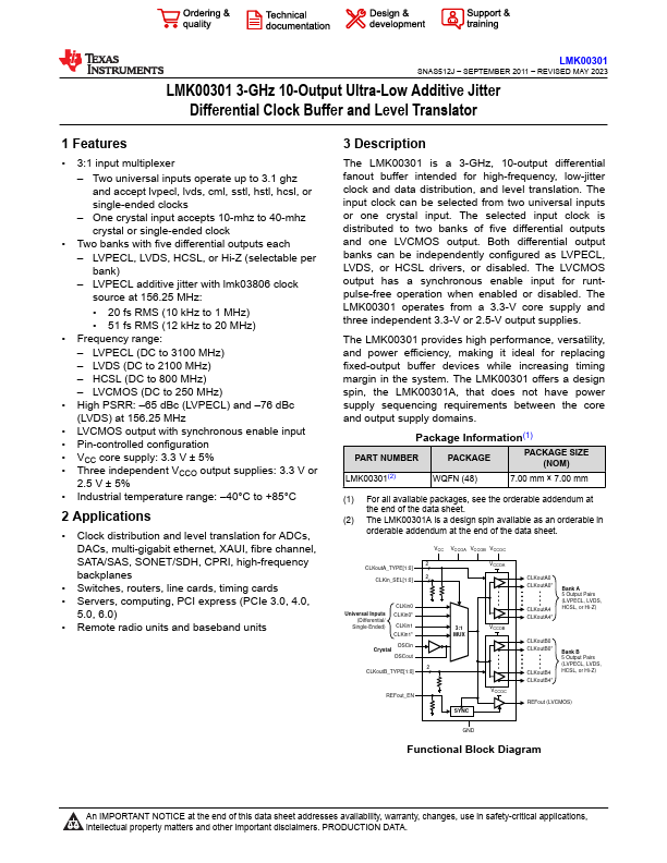
The LMK00301 is a 3-GHz, 10-output differential fanout buffer intended for high-frequency, low-jitter clock and data distribution, and level translation. The input clock can be selected from two universal inputs or one crystal input.
- 3:1 input multiplexer - Two universal inputs operate up to 3.1 ghz and accept lvpecl, lvds, cml, sstl, hstl, hcsl, or single-ended clocks - One crystal input accepts 10-mhz to 40-mhz crystal or single-ended clock
- Two banks with five differential outputs each - LVPECL, LVDS, HCSL, or Hi-Z (selectable per bank) - LVPECL additive jitter with lmk03806 clock source at 156.25 MHz:
- 20 fs RMS (10 kHz to 1 MHz)
- 51 fs RMS (12 kHz to 20 MHz)
- Frequency range: - LVPECL (DC to 3100 MHz) - LVDS (DC to 2100 MHz) - HCSL (DC to 800 MHz) - LVCMOS (DC to 250 MHz)
- High PSRR: -65 dBc (LVPECL) and -76 dBc (LVDS) at 156.25 MHz
- LVCMOS output with synchronous enable input
- Pin-controlled configuration
- VCC core supply: 3.3 V ± 5%
- Three independent VCCO output supplies: 3.3 V or 2.5 V ± 5%