LMK00308
Overview
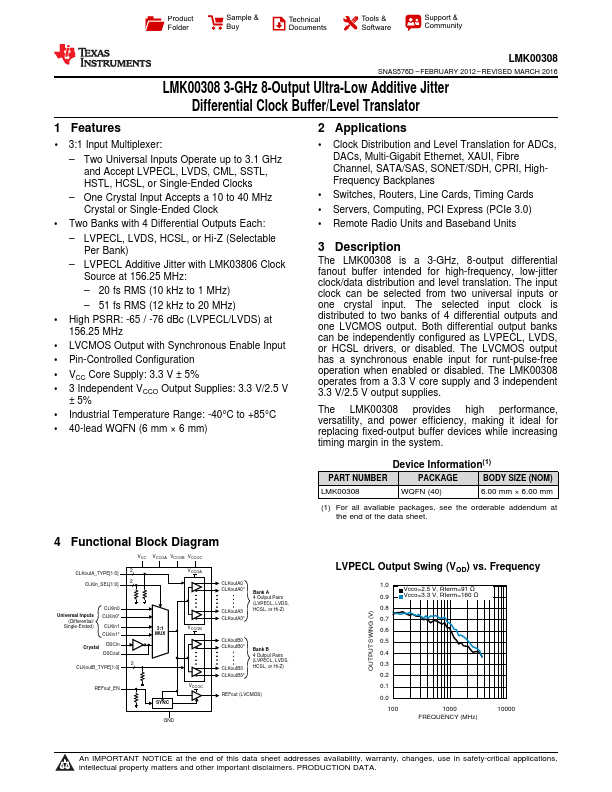
The LMK00308 is a 3-GHz, 8-output differential fanout buffer intended for high-frequency, low-jitter clock/data distribution and level translation. The input clock can be selected from two universal inputs or one crystal input.
- 1 3:1 Input Multiplexer: - Two Universal Inputs Operate up to 3.1 GHz and Accept LVPECL, LVDS, CML, SSTL, HSTL, HCSL, or Single-Ended Clocks - One Crystal Input Accepts a 10 to 40 MHz Crystal or Single-Ended Clock
- Two Banks with 4 Differential Outputs Each: - LVPECL, LVDS, HCSL, or Hi-Z (Selectable Per Bank) - LVPECL Additive Jitter with LMK03806 Clock Source at 156.25 MHz: - 20 fs RMS (10 kHz to 1 MHz) - 51 fs RMS (12 kHz to 20 MHz)
- High PSRR: -65 / -76 dBc (LVPECL/LVDS) at 156.25 MHz
- LVCMOS Output with Synchronous Enable Input
- Pin-Controlled Configuration
- VCC Core Supply: 3.3 V ± 5%
- 3 Independent VCCO Output Supplies: 3.3 V/2.5 V ± 5%
- Industrial Temperature Range: -40°C to +85°C
- 40-lead WQFN (6 mm × 6 mm)