SN74AHCT367
SN74AHCT367 is Hex Buffer and Line Driver manufactured by Texas Instruments.
Features
- 1 Inputs are TTL-Voltage patible
- True Outputs
- Latch-Up Performance Exceeds 100 m A
Per JESD 78, Class II
- ESD Protection Exceeds JESD 22
- 2000-V Human-Body Model
- 200-V Machine Model
- 2000-V Charged-Device Model
2 Applications
- Tele Infrastructure
- TVs
- Set Top Boxes
- Network Switches
- Wireless Infrastructure
- Electronic Points of Sale
3 Description
The SN74AHCT367 device is designed specifically to improve both the performance and density of 3-state memory address drivers, clock drivers, and bus-oriented receivers and transmitters.
Device Information(1)
PART NUMBER
PACKAGE
BODY SIZE (NOM)
PDIP (16)
19.30 mm x 6.35 mm
SSOP (16)
6.50 mm x 5.30 mm
TSSOP (16)
5.00 mm x 4.40 mm
SOP (16)
10.20 mm x 5.30 mm
SOIC (16)
9.00 mm x 3.90 mm
(1) For all available packages, see the orderable addendum at the end of the data sheet.
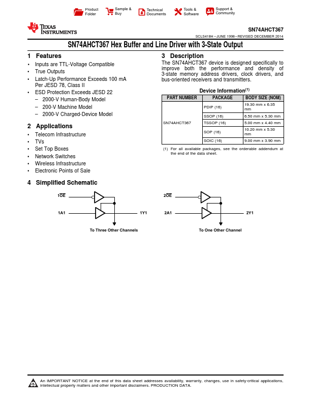
4 Simplified Schematic
1OE
2OE
1A1
1Y1
2A1
2Y1...