SN74ALVC126
FEATURES
- Operates From 1.65 V to 3.6 V
- Max tpd of 3.1 ns at 3.3 V
- ±24-m A Output Drive at 3.3 V
- Latch-Up Performance Exceeds 250 m A Per
JESD 17
- ESD Performance Tested Per JESD 22
- 2000-V Human-Body Model (A114-A)
- 200-V Machine Model (A115-A)
- 1000-V Charged-Device Model (C101)
SN74ALVC126 QUADRUPLE BUS BUFFER GATE
WITH 3-STATE OUTPUTS
SCES111J
- JULY 1997
- REVISED OCTOBER 2004
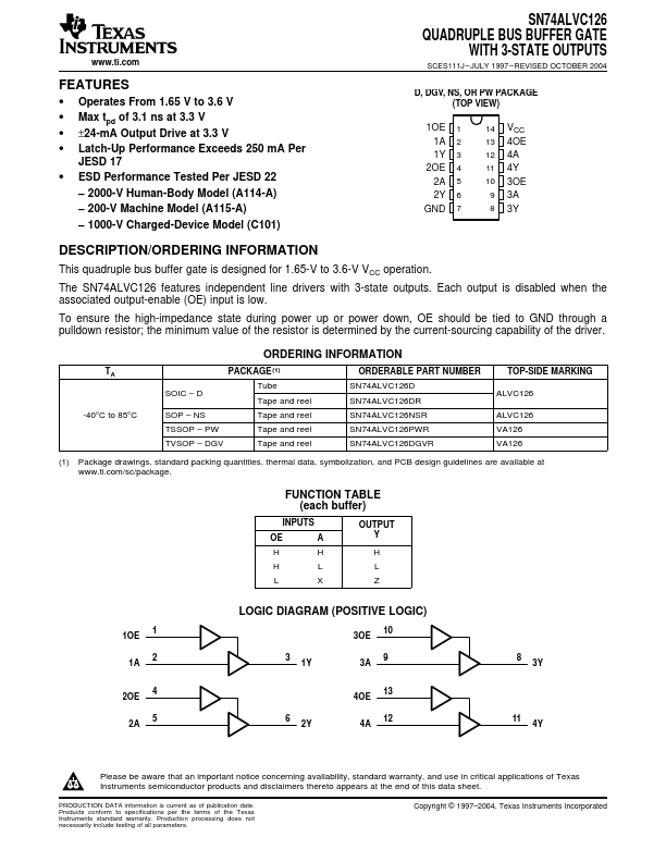
D, DGV, NS, OR PW PACKAGE (TOP VIEW)
1OE 1 1A 2 1Y 3
2OE 4 2A 5 2Y 6
GND 7
14 VCC 13 4OE 12 4A 11 4Y 10 3OE 9 3A 8 3Y
DESCRIPTION
/ORDERING INFORMATION
This quadruple bus buffer gate is designed for 1.65-V to 3.6-V VCC operation. The SN74ALVC126 features independent line drivers with 3-state outputs. Each output is disabled when the associated output-enable (OE) input is low.
To ensure the high-impedance state during power up or power down, OE should be tied to GND through a pulldown resistor; the minimum value of the resistor is determined by the current-sourcing capability of the driver.
TA...