SN74AS885 Overview
Key Specifications
Package: SOIC
Mount Type: Surface Mount
Pins: 24
Operating Voltage: 5 V
Description
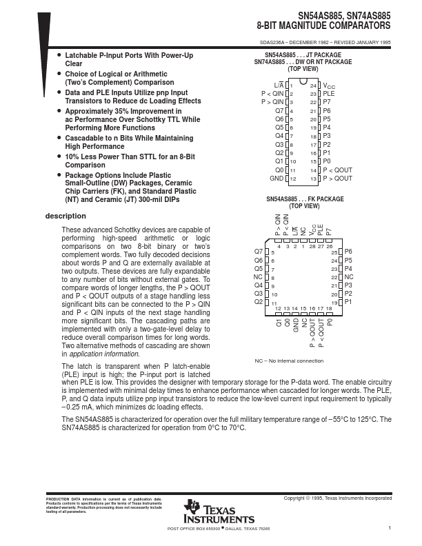
SDAS236A – DECEMBER 1982 – REVISED JANUARY 1995 SN54AS885. JT PACKAGE SN74AS885.
| Part | SN74AS885 |
|---|---|
| Description | 8-BIT MAGNITUDE COMPARATORS |
| Category | Comparator |
| Manufacturer | Texas Instruments |
| Size | 391.98 KB |
Package: SOIC
Mount Type: Surface Mount
Pins: 24
Operating Voltage: 5 V
SDAS236A – DECEMBER 1982 – REVISED JANUARY 1995 SN54AS885. JT PACKAGE SN74AS885.
| Seller | Inventory | Price Breaks | Buy |
|---|---|---|---|
| Rochester Electronics | 6497 | 25+ : 14.18 USD 100+ : 13.47 USD 500+ : 12.76 USD 1000+ : 12.05 USD |
View Offer |
| DigiKey | 3 | 1+ : 22.56 USD | View Offer |
| Part Number | Manufacturer | Description |
|---|---|---|
| LM393 | STMicroelectronics | Low-power dual-voltage comparators |
| CMP401 | Analog Devices | Low Voltage Comparators |
| CMP402 | Analog Devices | Low Voltage Comparators |