Datasheet Details
| Part number | SN74F175 |
|---|---|
| Manufacturer | Texas Instruments |
| File Size | 887.63 KB |
| Description | QUADRUPLE D-TYPE FLIP-FLOP |
| Datasheet | SN74F175-etcTI.pdf |
|
|
|
Overview: D Contains Four Flip-Flops With Double-Rail Outputs D Buffered Clock and Direct Clear Inputs D Applications Include: – Buffer/Storage Registers – Shift Registers – Pattern.
| Part number | SN74F175 |
|---|---|
| Manufacturer | Texas Instruments |
| File Size | 887.63 KB |
| Description | QUADRUPLE D-TYPE FLIP-FLOP |
| Datasheet | SN74F175-etcTI.pdf |
|
|
|
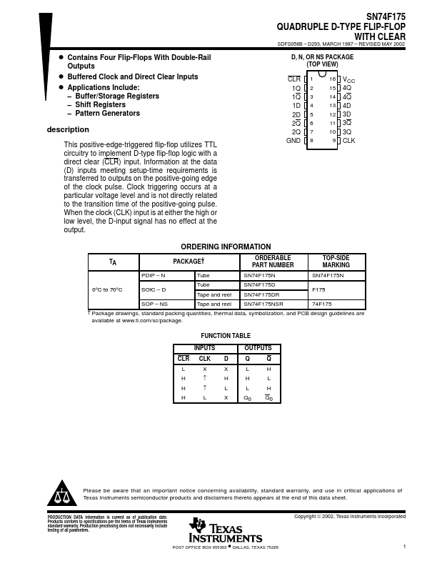
This positive-edge-triggered flip-flop utilizes TTL circuitry to implement D-type flip-flop logic with a direct clear (CLR) input.
Information at the data (D) inputs meeting setup-time requirements is transferred to outputs on the positive-going edge of the clock pulse.
Clock triggering occurs at a particular voltage level and is not directly related to the transition time of the positive-going pulse.
| Part Number | Description |
|---|---|
| SN74F174A | HEX D-TYPE FLIP-FLOP |
| SN74F10 | TRIPLE 3-INPUT POSITIVE-NAND GATE |
| SN74F1016 | 16-Bit Schottky Barrier Diode RC Bus-Termination Array |
| SN74F1056 | 8-BIT SCHOTTKY BARRIER DIODE BUS-TERMINATION ARRAY |
| SN74F109 | DUAL J-K POSITIVE-EDGE-TRIGGERED FLIP-FLOP |
| SN74F11 | Triple 3-Input AND Gate |
| SN74F112 | DUAL NEGATIVE-EDGE-TRIGGERED J-K FLIP-FLOP |
| SN74F125 | QUADRUPLE BUS BUFFER GATE |
| SN74F126 | QUADRUPLE BUS BUFFER GATE |
| SN74F138 | 3-LINE TO 8-LINE DECODERS/DEMULTIPLEXERS |