SN74LV125A
Overview
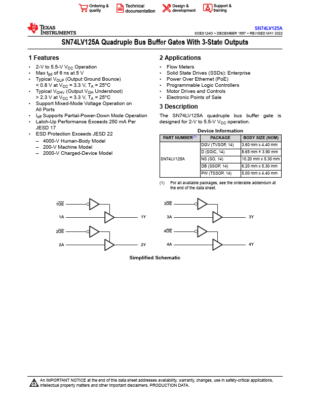
The SN74LV125A quadruple bus buffer gate is designed for 2-V to 5.5-V VCC operation. Device Information PART NUMBER(1) PACKAGE BODY SIZE (NOM) DGV (TVSOP, 14) 3.60 mm x 4.40 mm D (SOIC, 14) 8.65 mm × 3.90 mm SN74LV125A NS (SO, 14) 10.20 mm x 5.30 mm DB (SSOP, 14) 6.20 mm x 5.30 mm PW (TSSOP, 14) 5.00 mm x 4.40 mm (1) For all available packages, see the orderable addendum at the end of the data sheet. 1OE 3OE 1A 1Y 3A 3Y 2OE 4OE 2A 2Y 4A 4Y Simplified Schematic An IMPORTANT NOTICE at the end of this data sheet addresses availability, warranty, changes, use in safety-critical applications, intellectual property matters and other important disclaimers.
- 2-V to 5.5-V VCC Operation
- Max tpd of 6 ns at 5 V
- Typical VOLP (Output Ground Bounce) < 0.8 V at VCC = 3.3 V, TA = 25°C
- Typical VOHV (Output VOH Undershoot) > 2.3 V at VCC = 3.3 V, TA = 25°C
- Support Mixed-Mode Voltage Operation on All Ports
- Ioff Supports Partial-Power-Down Mode Operation
- Latch-Up Performance Exceeds 250 mA Per JESD 17
- ESD Protection Exceeds JESD 22 - 4000-V Human-Body Model - 200-V Machine Model - 2000-V Charged-Device Model