• Part: SN74LV595A-Q1
  • Description: 8-Bit Shift Registers
  • Manufacturer: Texas Instruments
  • Size: 841.08 KB
Download SN74LV595A-Q1 Datasheet PDF
Texas Instruments
SN74LV595A-Q1
SN74LV595A-Q1 is 8-Bit Shift Registers manufactured by Texas Instruments.
.ti. SCLS539D - AUGUST 2003 - REVISED OCTOBER 2009 8-BIT SHIFT REGISTER WITH 3-STATE OUTPUT REGISTERS Check for Samples: SN74LV595A-Q1 Features - Qualified for Automotive Applications - Customer-Specific Configuration Control Can Be Supported Along With Major-Change Approval - 2-V to 5.5-V VCC Operation - Typical VOLP (Output Ground Bounce) < 0.8 V at VCC = 3.3 V, TA = 25°C - Typical VOHV (Output VOH Undershoot) > 2.3 V at VCC = 3.3 V, TA = 25°C - Supports Mixed-Mode Voltage Operation on All Ports - 8-Bit Serial-In, Parallel-Out Shift - Ioff Supports Partial-Power-Down Mode Operation - Shift Register Has Direct Clear QB QC QD QE QF QG QH GND 1 2 3 4 5 6 7 8 16 VCC 15 QA 14 SER 13 OE 12 RCLK 11 SRCLK 10 SRCLR 9 QH′ DESCRIPTION 
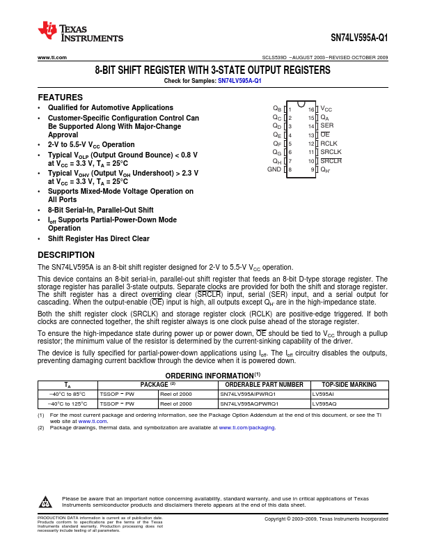
The SN74LV595A is an 8-bit shift register designed for 2-V to 5.5-V VCC operation. This device contains an 8-bit serial-in, parallel-out shift register that feeds an 8-bit D-type storage register. The storage register has parallel 3-state outputs. Separate clocks are provided for both the shift and storage register. The shift register has a direct overriding clear (SRCLR) input, serial (SER) input, and a serial output for cascading. When the output-enable (OE) input is high, all outputs except QH' are in the high-impedance state. Both the shift register clock (SRCLK) and storage register clock (RCLK) are positive-edge triggered. If both clocks are connected together, the shift register always is one clock pulse ahead of the storage register. To ensure the high-impedance state during power up or power down, OE should be tied to VCC through a pullup resistor; the minimum value of the resistor is determined by the current-sinking capability of the driver. The device is fully specified for partial-power-down applications using Ioff. The Ioff circuitry disables the outputs, preventing damaging current backflow through the device when it is powered down. - 40°C to 85°C - 40°C to 125°C TSSOP - PW...