SN74LVC2G126-EP Overview
Description
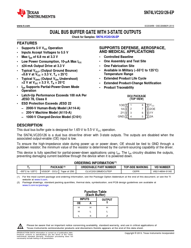
This dual bus buffer gate is designed for 1.65-V to 5.5-V VCC operation. The SN74LVC2G126 is a dual bus driver/line driver with 3-state outputs.
Key Features
- Supports 5-V VCC Operation
- Inputs Accept Voltages to 5.5 V
- Max tpd of 6.8 ns at 3.3 V
- Low Power Consumption, 10-μA Max ICC
- ±24-mA Output Drive at 3.3 V
- Typical VOLP (Output Ground Bounce) <0.8 V at VCC = 3.3 V, TA = 25°C
- Typical VOHV (Output VOH Undershoot) >2 V at VCC = 3.3 V, TA = 25°C
- Ioff Supports Partial-Power-Down Mode Operation
- Latch-Up Performance Exceeds 100 mA Per JESD 78, Class II
- Controlled Baseline