Datasheet4U Logo Datasheet4U.com

SN74LVC2G126 - Dual Bus Buffer Gate

Datasheet Summary

Description

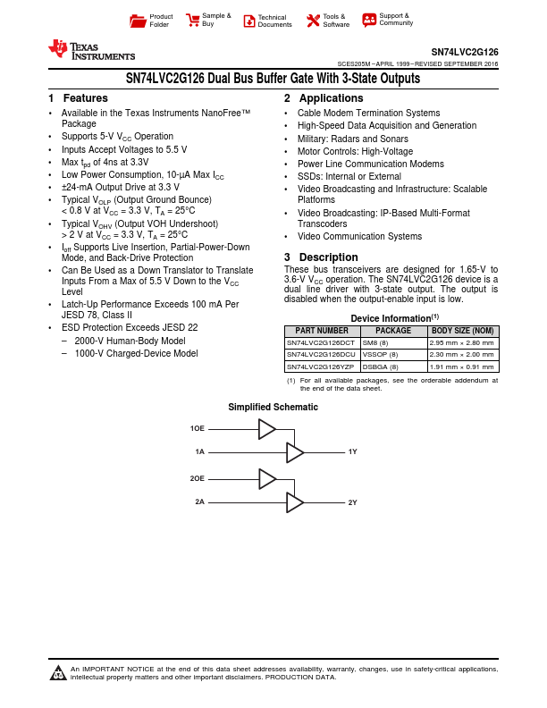
These bus transceivers are designed for 1.65-V to 3.6-V VCC operation.

The SN74LVC2G126 device is a dual line driver with 3-state output.

The output is disabled when the output-enable input is low.

Features

  • 1 Available in the Texas Instruments NanoFree™ Package.
  • Supports 5-V VCC Operation.
  • Inputs Accept Voltages to 5.5 V.
  • Max tpd of 4ns at 3.3V.
  • Low Power Consumption, 10-µA Max ICC.
  • ±24-mA Output Drive at 3.3 V.
  • Typical VOLP (Output Ground Bounce) < 0.8 V at VCC = 3.3 V, TA = 25°C.
  • Typical VOHV (Output VOH Undershoot) > 2 V at VCC = 3.3 V, TA = 25°C.
  • Ioff Supports Live Insertion, Partial-Power-Down Mode, and Back-Drive.

📥 Download Datasheet

Datasheet preview – SN74LVC2G126

Datasheet Details

Part number SN74LVC2G126
Manufacturer Texas Instruments
File Size 1.01 MB
Description Dual Bus Buffer Gate
Datasheet download datasheet SN74LVC2G126 Datasheet
Additional preview pages of the SN74LVC2G126 datasheet.
Other Datasheets by Texas Instruments

Full PDF Text Transcription

Click to expand full text
Product Folder Sample & Buy Technical Documents Tools & Software Support & Community SN74LVC2G126 SCES205M – APRIL 1999 – REVISED SEPTEMBER 2016 SN74LVC2G126 Dual Bus Buffer Gate With 3-State Outputs 1 Features •1 Available in the Texas Instruments NanoFree™ Package • Supports 5-V VCC Operation • Inputs Accept Voltages to 5.5 V • Max tpd of 4ns at 3.3V • Low Power Consumption, 10-µA Max ICC • ±24-mA Output Drive at 3.3 V • Typical VOLP (Output Ground Bounce) < 0.8 V at VCC = 3.3 V, TA = 25°C • Typical VOHV (Output VOH Undershoot) > 2 V at VCC = 3.3 V, TA = 25°C • Ioff Supports Live Insertion, Partial-Power-Down Mode, and Back-Drive Protection • Can Be Used as a Down Translator to Translate Inputs From a Max of 5.
Published: |