TS3DDR32611
TS3DDR32611 is 1A Peak Sink/Source PCDDR3 Termination Regulator manufactured by Texas Instruments.
FEATURES
- VDD Range
- 3.0V to 3.6V
- RON 1.75Ω typical
- Channel Count
- 26
- VDDQ
- Input Voltage 1.2V to 3.5V
- VTT
- VDDQ/2 typical with 1A sink/source capability
- VREF
- VDDQ/2±1% × VDDQ
- Switch Time
- (TON/OFF) 100ns Max
- IDD Supply Current
- High Speed Mode (IDD,HS) 220 µA Max
- Low Speed Mode (IDD,LS) 220 µA Max
- Power Down Mode (IDD,PD) 5 µA Max
- Special Features
- 1.8-V patible Control Inputs (VTT_EN,
ODT_EN)
- High current Sinking/Sourcing Capability:
1A Max
- 48-Ball ZQC Package (4mm x 4mm, 0.5mm pitch)
APPLICATIONS
- Double Data Rate type 3 (PCDDR3) termination and regulation in mobile devices
DESCRIPTION
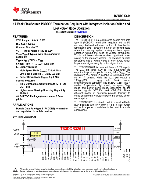
The TS3DDR32611 is a sink/source double data rate type III (PCDDR3) termination regulator with a 1% accuracy buffered reference output. It has built-in termination SPST switches that can be disconnected when the memory system undergoes lower speed operation without the need of voltage termination. Turning off these switches enables significant power saving on the memory system. The switches on-state resistance has a typical value of only 1.75Ω which helps retain signal integrity on the signal lines.
The TS3DDR32611 is powered from a 3.3V supply. The VDDQ pin takes 1.2V to 1.8V input while the output voltage at VTT pin is tracking 1/2 × VDDQ. The regulator’s VTT output is capable of sinking/sourcing up to 1A current, while the VREF pin output is 1/2VDDQ±1% × VDDQ with 5m A current sinking/sourcing capability. The TS3DDR32611 has 4 modes of operation: high speed, low speed, VREF mode and power down mode, depending on the control signals VTT_EN and ODT_EN. These different modes of operation provide flexibility to establish a memory system’s performance and power consumption.
The TS3DDR32611 is situated within a small 48 balls BGA package with only 4mm x 4mm in size, which makes it a perfect candidate to be used in mobile applications.
SWITCH DIAGRAM
VLDOIN VDDQ
3.3V Supply
VTT Regulator
VTT_EN OBT_EN
VDD GND
VREF VTT...