NP6667SR
Description
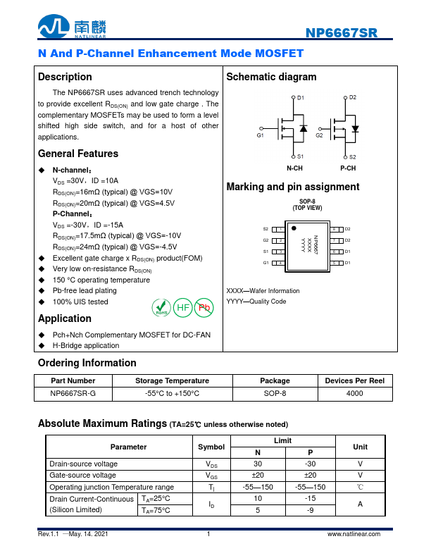
Schematic diagram
The NP6667SR uses advanced trench technology to provide excellent RDS(ON) and low gate charge . The plementary MOSFETs may be used to form a level shifted high side switch, and for a host of other applications.
General Features
- N-channel:
VDS =30V,ID =10A
RDS(ON)=16mΩ (typical) @ VGS=10V
RDS(ON)=20mΩ (typical) @ VGS=4.5V P-Channel:
VDS =-30V,ID =-15A
RDS(ON)=17.5mΩ (typical) @ VGS=-10V
RDS(ON)=24mΩ (typical) @ VGS=-4.5V
- Excellent gate charge x RDS(ON) product(FOM)
- Very low on-resistance RDS(ON)
- 150 °C operating temperature
- Pb-free lead plating
- 100% UIS tested
HF Pb
Application
N-CH
P-CH
Marking and pin assignment
SOP-8 (TOP VIEW)
S2
G2
S1
G1
NP6667 XXXX YYYY
8 D2
D2
D1
5 D1
XXXX- Wafer Information YYYY- Quality Code
- Pch+Nch plementary MOSFET for DC-FAN
- H-Bridge...