Nexperia 74HC107D
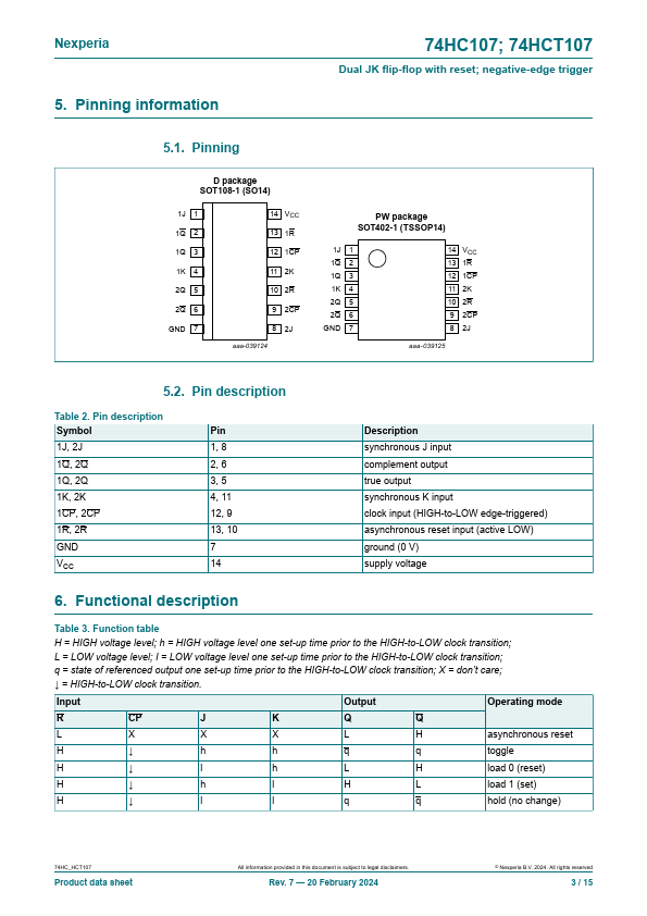
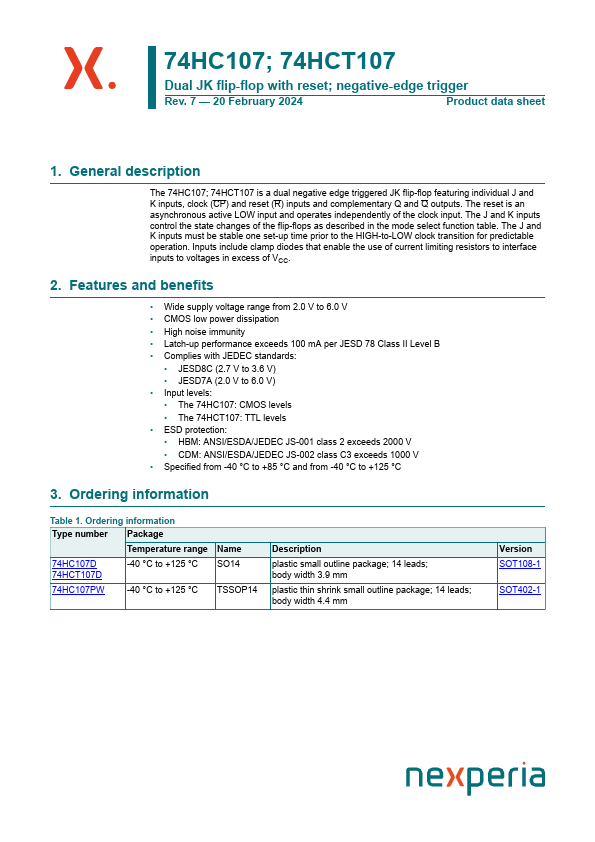
The 74HC107; 74HCT107 is a dual negative edge triggered JK flip-flop featuring individual J and K inputs, clock (CP) and reset (R) inputs and complementary Q and Q outputs. The reset is an asynchronous active LOW input and operates independently of the clock input. The J and K inputs control the state changes of the flip-flops as described in the mode select function table.| Part No. | 74HC107D |
|---|---|
| Datasheet | 74HC107D Download |
| Manufacturer |  Nexperia |
| Description | Dual JK flip-flop |
| Buy | Stock & Price |
FEATURES AND BENEFITS
● Wide supply voltage range from 2.0 V to 6.0 V● CMOS low power dissipation
● High noise immunity
● Latch-up performance exceeds 100 mA per JESD 78 Class II Level B
● Complies with JEDEC standards:
● JESD8C (2.7 V to 3.6 V)
● JESD7A (2.0 V to 6.0 V)
● Input levels:
● The 74HC107: CMOS levels
● The 74HCT107: TTL levels
● ESD protection:
● HBM: ANSI/ESDA/JEDEC JS-001 class 2 exceeds 2000 V
● CDM: ANSI/ESDA/JEDEC JS-002 class C3 exceeds 1000 V
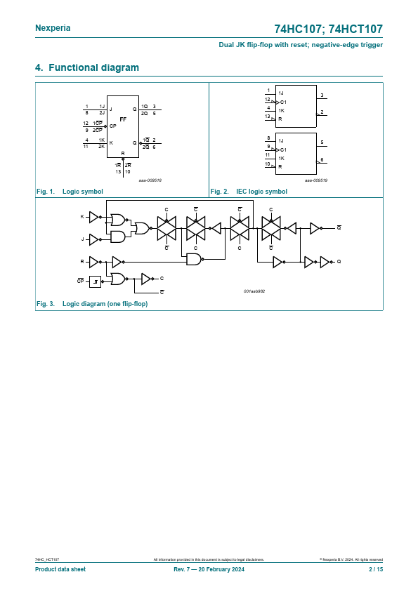
● Specified from -40 °C to +85 °C and from -40 °C to +125 °C 3. Ordering information Table 1. Ordering information Type number Package Temperature range Name 74HC107D 74HCT107D -40 °C to +125 °C SO14 74HC107PW -40 °C to +125 °C TSSOP14
DESCRIPTION
plastic small outline package; 14 leads; body width 3.9 mm plastic thin shrink small outline package; 14 leads; body width 4.4 mm Version SOT108-1 SOT402-1 Nexperia 4. Functional diagram 1 8 1J 2J J Q 1Q 3 2Q 5 12 1CP FF CP 9 2CP 4 11 1K 2K K Q 1Q 2 2Q 6 R Fig. 1. Logic symbol 1R 2R 13 10 aaa-009518 C K J C R CP C C Fig.