Datasheet4U Logo Datasheet4U.com

74LV08D - Quad 2-input AND gate

Download the 74LV08D datasheet PDF. This datasheet also covers the 74LV08 variant, as both devices belong to the same quad 2-input and gate family and are provided as variant models within a single manufacturer datasheet.

General Description

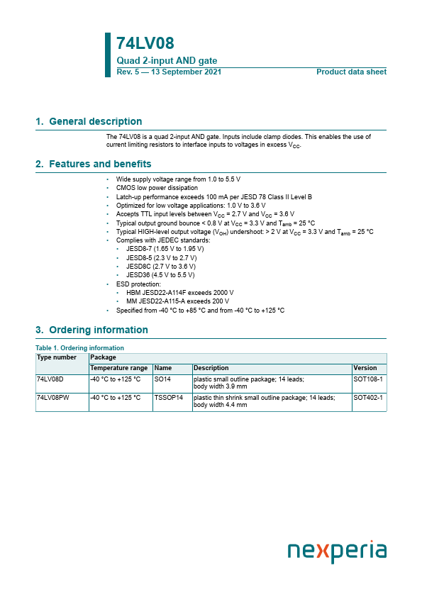
The 74LV08 is a quad 2-input AND gate.

Inputs include clamp diodes.

This enables the use of current limiting resistors to interface inputs to voltages in excess VCC.

Key Features

  • Wide supply voltage range from 1.0 to 5.5 V.
  • CMOS low power dissipation.
  • Latch-up performance exceeds 100 mA per JESD 78 Class II Level B.
  • Optimized for low voltage.

📥 Download Datasheet

Note: The manufacturer provides a single datasheet file (74LV08-nexperia.pdf) that lists specifications for multiple related part numbers.

Datasheet Details

Part number 74LV08D
Manufacturer Nexperia
File Size 213.45 KB
Description Quad 2-input AND gate
Datasheet download datasheet 74LV08D Datasheet

Full PDF Text Transcription (Reference)

The following content is an automatically extracted verbatim text from the original manufacturer datasheet and is provided for reference purposes only.

View original datasheet text
74LV08 Quad 2-input AND gate Rev. 5 — 13 September 2021 Product data sheet 1. General description The 74LV08 is a quad 2-input AND gate. Inputs include clamp diodes. This enables the use of current limiting resistors to interface inputs to voltages in excess VCC. 2. Features and benefits • Wide supply voltage range from 1.0 to 5.5 V • CMOS low power dissipation • Latch-up performance exceeds 100 mA per JESD 78 Class II Level B • Optimized for low voltage applications: 1.0 V to 3.6 V • Accepts TTL input levels between VCC = 2.7 V and VCC = 3.6 V • Typical output ground bounce < 0.8 V at VCC = 3.3 V and Tamb = 25 °C • Typical HIGH-level output voltage (VOH) undershoot: > 2 V at VCC = 3.3 V and Tamb = 25 °C • Complies with JEDEC standards: • JESD8-7 (1.65 V to 1.95 V) • JESD8-5 (2.