onsemi 2N7002KW
N-Channel FET
| Part No. | 2N7002KW |
|---|---|
| Datasheet | 2N7002KW Download |
| Manufacturer |  onsemi |
| Description | N-Channel FET |
| Buy | Stock & Price |
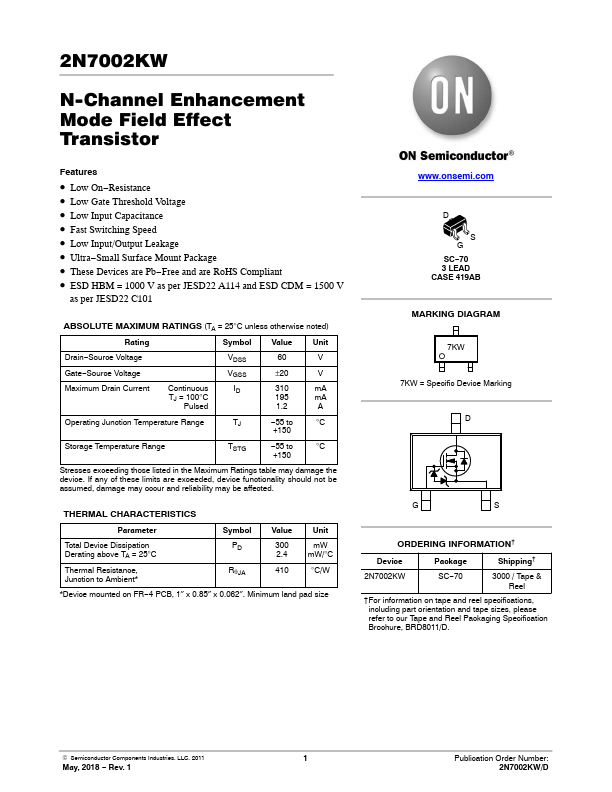
FEATURES
● Low On−Resistance● Low Gate Threshold Voltage
● Low Input Capacitance
● Fast Switching Speed
● Low Input/Output Leakage
● Ultra−Small Surface Mount Package
● These Devices are Pb−Free and are RoHS Compliant
● ESD HBM = 1000 V as per JESD22 A114 and ESD CDM = 1500 V as per JESD22 C101
ABSOLUTE MAXIMUM RATINGS
(TA = 25°C unless otherwise noted) Rating Symbol Value Unit Drain−Source Voltage Gate−Source Voltage Maximum Drain Current Continuous TJ = 100°C Pulsed VDSS VGSS ID 60 V ±20 V 310 mA 195 mA 1.2 A Operating Junction Temperature Range TJ −55 to °C +150 Storage Temperature Range TSTG −55 to °C +150 Stresses exceeding those listed in theMAXIMUM RATINGS
table may damage the device. If any of these limits are exceeded, device functionality should not be assumed, damage may occur and reliability may be affected. THERMAL CHARACTERISTICS Parameter Symbol Value Unit Total Device Dissipation Derating above TA = 25°C Thermal Resistance, Junction to Ambient* PD RqJA 300 mW 2.4 mW/°C 410 °C/W *Device mounted on FR−4 PCB, 1″ x 0.85″ x 0.062″.
